0 Preface
Since its inception, monolithic switching power supplies have quickly occupied an important position in the field of small and medium power precision regulated power supplies due to their high efficiency, small size, high integration and stable functions. The TOPSwitch series of American PI company is a new type of three-terminal off-line single-chip high-frequency switching power supply chip with a switching frequency of up to 100 kHz. This chip integrates PWM controller, high withstand voltage power MOSFET and protection circuit. A few devices can be connected to the peripheral. This paper introduces a principle and method for designing a single-ended flyback switching power supply based on TOP223Y output of +5 V/3 A, +12 V/1 A.
1 Principle of scheme design
Switching power supply is an application field involving many disciplines. AC/DC or DC/DC conversion can be realized by controlling the power-switching device to turn on and off to adjust the pulse width modulation duty ratio to achieve stable output.
TOP223Y has three terminals: control terminal C, source S, and drain D. Since only drain D is used as the pulse width modulation power control output, it is called single-ended; high-frequency transformer only stores energy when the power switch is turned on. In the primary winding, it acts as an inductor, and when the power switch is turned off, the energy is transmitted to the secondary winding, which acts as a transformer, so it is called a flyback type.

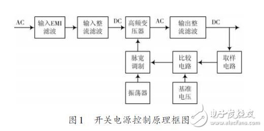
The circuit function part is mainly composed of input/output rectification filtering, power conversion and feedback circuit. The working principle is as follows: 220 V mains AC is rectified and filtered to obtain DC voltage, and then high frequency rectangular wave voltage is obtained by TOP223Y pulse width modulation and high frequency transformer DC-AC conversion. Finally, the output is rectified and filtered to obtain high quality DC voltage. At the same time, the feedback loop inputs the current signal to the control terminal C of the TOP223Y by sampling, comparing and amplifying the output voltage, and controls the duty ratio adjustment output to stabilize the output voltage.
2 Program design requirements
Designed as the power supply for a smart instrument, the specific parameters are as follows: AC input voltage minimum: VACMIN = 85 V; AC input voltage maximum: VACMAX = 265 V; output: U1: +5 V / 3 A; U2: +12 V/1 A; output power: Po=27 W; bias voltage: VB=12 V; grid frequency fL=50 Hz; switching frequency fs=100 kHz; ripple voltage: less than 100 mV; power efficiency: η More than 80%; loss distribution factor Z is 0.5; power factor is 0.5.
3 design examples
This design scheme is based on TOP223Y multi-channel single-ended flyback switching power supply, which has superior performance and is easy to integrate. The circuit principle is shown in Figure 2. It can be divided into input protection circuit, input rectification filter circuit, clamp protection circuit, high frequency transformer, output rectification filter circuit, feedback loop and control circuit.

3.1 Input protection circuit
It consists of fuse F1, thermistor RT and varistor RV, and protects the input terminal from overvoltage and overcurrent.
Fuse F1 is used to cut off the circuit when the line is faulty and overcurrent, the protection circuit components are not damaged, and its rated current IF1 selects 3 A/250 VAC fuse according to IF1》2IACRMS, where IACRMS is the primary effective current value. The thermistor RT is used to absorb the starting surge current, avoiding the transient current being too large, causing impact on the rectifier diode and the fuse, causing damage. Adding the thermistor can effectively improve the safety factor of the power supply design, and its resistance is in accordance with RRT1 <<0.01 VACMAX/IACRMS selects 10D-11 (10 Ω/2.4 A). The varistor RV provides a discharge path when the AC input is disconnected to prevent large current surges and also has a good clamping effect on the surge voltage. RV selects MY31-270/3, nominally 220 V.
3.2 Input rectification filter circuit
It consists of EMI filter circuit, rectifier circuit and voltage regulator circuit.
The EMI filter circuit is for noise interference from the power grid. A typical Î -type filter composed of L1, CX1, CX2, CY1, and CY2 is used.
CX1 and CX2 are used to filter differential mode interference from the power grid, called X capacitor, usually 100~220 nF, here 100 μF; CY1 and CY2 are used to filter common mode interference from the power grid, called Y capacitor Usually, the value is 1~4.7 nF, which is 2.2 nF. The common mode inductance L1 used to eliminate common mode interference is 8~33 mH, where 8 mH is taken, and the double line is wound.
The input rectifier circuit selects an uncontrollable full-wave rectifier bridge. The reverse withstand voltage of the rectifier bridge should be greater than 1.25 times the maximum DC input voltage. The rated current of the rectifier bridge should be greater than twice the effective value of the AC input. After calculation, the reverse breakdown voltage is 560 V and the rated current is 3. A KBP306 rectifier bridge.
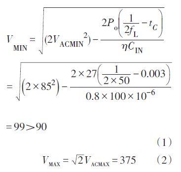
Under the current power supply conditions, the value of the input storage capacitor CIN is taken according to the output power according to 2~3 μF/W. Considering the margin, take the Electrolytic capacitor of CIN=100 μF/400 V. Assume that the diode conduction time in the rectifier bridge is tc=3 ms, which can be:

Get the minimum and maximum values ​​of the input DC voltage.
Other capacitors
Ac Filter Capacitor,Power Saver Capacitor,Line Filter Capacitor,Low Voltage Capacitor
YANGZHOU POSITIONING TECH CO., LTD , https://www.yzpstcc.com