The inverter system is a typical interdependent, intricate hybrid system [6]. The code programming of the traditional DSP system is time-consuming and labor-intensive. Mathworks and TI jointly launched the TSP tool to enable embedded system modeling, simulation, code generation and debugging in the Simulink environment, greatly improving engineering development efficiency. This article implements automatic code generation on the inverter system.
1 code generation technology
Automatic code generation technology refers to the use of specific software (MATLAB) or a specific toolbox in the software to build a system simulation model of the target code, and automatically generate an embedded system application according to a specific target configuration [7-8].
Embedded Coder is a powerful tool that MathWorks provides to Simulink users for embedded systems development. TSP TI C2000 (Embedded Coder Target Support Package for Texas Instruments C2000 Processors) toolbox is jointly developed by TI and MathWorks, and can be seamlessly interfaced with TI's CCS (Coder Composer Studio) integrated development environment (IDE). Toolbox for C2000 series DSP embedded system development [9-10]. The toolkit provides a one-to-one interface module for DSP peripheral resources that transforms the system model into optimizable, portable, custom, product-level embedded C code [11-12]. The model source and signal receiving part modules are replaced with I/O ports. The system.tlc file provided by the software is responsible for coordinating the entire process of calling code generation, and automatically generating system applications according to the target configuration.
Application code generation technology does not require the code required for model simulation to be written line by line, and it is easier to debug accordingly. Compared with the traditional design method, it has obvious characteristics of short development cycle, low cost and high efficiency.
2 Development process based on code generation technology
Firstly, the system design standard is determined according to the requirements. The system simulation model is established according to the design idea in the Simulink platform. Secondly, the model parameters and the simulation environment are set according to the system design requirements, and the corresponding intelligent algorithms are implanted. After the configuration work is completed, the model simulation is performed. The simulation results were observed in real time during the simulation. If the simulation results deviate from the expected results, the simulation model or parameter settings are improved in time and repeated corrections until the simulation results are consistent with the theoretical results. After the simulation is completed, configure the target environment for the Simulink model, set the system file and hardware debugging environment, compile the code generation model, generate the code execution file (.out), connect the hardware debugging board, download the execution file, run the program, observe and test the system parameters. . The development process is shown in Figure 1.
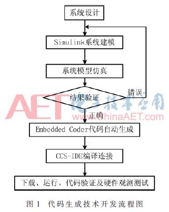
3 three-level inverter
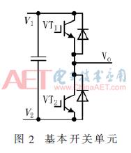
The three-level inverter is a common power electronic circuit topology, which is formed by a series-parallel topology with a bridge arm of a two-level converter as the basic switching unit [13], and the basic switching unit is the structure of FIG. Only two levels are output, which are combined in series or in parallel by the basic switching unit to achieve a voltage value of more than two voltage levels outputted at the output. A single-phase bridge arm of a three-level inverter as shown in FIG. 3 can be constructed, and three identical bridge arms are connected in parallel and combined with a necessary device such as a DC power supply to obtain a three-level full-bridge inverter structure.
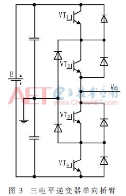
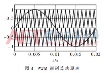
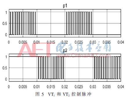
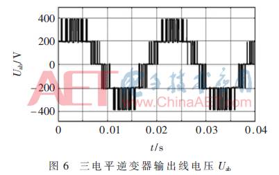
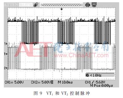
The IGBT on the bridge arm is controlled in an orderly manner according to the modulation algorithm law, so that the IGBT works according to the inherent law, and the three-level full-bridge AC voltage wave can be output. The modulation algorithm is shown in Figure 4. The positive half-axis carrier and the modulated wave generate complementary two-column trigger pulses, respectively triggering VT1 and VT3; the negative half-axis carrier and the modulated wave generate complementary two-column trigger pulses, respectively triggering VT2 and VT4 . The control pulses p1 and p2 of VT1 and VT2 are as shown in FIG. The output line voltage Uab is shown in Fig. 6. Compared with the conventional two-level inverter, the withstand voltage and capacity of the three-level inverter power tube are doubled, and the du/dt of the output line voltage is reduced. Significantly improved, the contrast is closer to a sine wave than the two-level line voltage.
4 three-level PWM code generation
The three-level PWM is a 12-way trigger pulse. If the program is written line by line in CCS, it is a very large task, and inevitably there will be errors during the programming process. It is necessary to constantly modify and test the code. It takes a lot of manpower. In order to save manpower and time, reduce error rate, and improve development efficiency, automatic code generation technology is used to generate three-level PWM control pulses. Establish a three-level PWM automatic code generation model as shown in Figure 7.
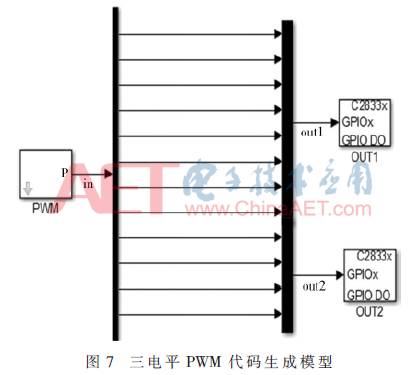
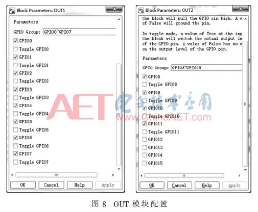
The TSP toolbox only provides the peripheral interface of the DSP. It is necessary to build a three-level PWM model using other Simulink tools, and then define the output port [14-15] by the Digital Output module in the TSP. The PWM module is from Simulink>Power Systems>SpecializedTechnology>Control&Measurements>Pulse&Signal Generators. This module is a three-level PWM output module, setting parameters such as frequency, phase and sampling period to make the inverter output voltage 50 Hz. The three-level PWM output has 12 pulses, and each Digital Output module provides only 8 GPIO interfaces. It needs to be combined with the Demux and Mux modules to output pulses with two Digital Output modules. In Figure 7, the OUT1 module GPIO0~GPIO7 are set to use, and the OUT2 module GPIO8~GPIO11 is used. As shown in Figure 8, a total of 12 pulses are used to control the IGBT operation.
After the model is successfully established, set the target environment. Open the Simulation>Model Configuration Parameter environment configuration, set the simulation environment to discrete environment in Solver, set the TI Delfino F2833x target board for Hardware Implementation>Hardware board, set the ert.tlc system file in Code Generation>System target file, and select CCS development environment for Toolchain. TI CCSV6 C2000, Interface>Code replacement library is set to TI C28x. Code Optimization > File packaging format is set to Compact, which optimizes the logical structure of the generated code and improves the readability of the code.
After the above modeling and target environment configuration is completed, press Ctrl+B to combine the shortcut keys to compile the model, or find the compilation tool in the model toolbar and click the edit model. If the model design and environment configuration are correct, the .out executable file can be generated. The file can be downloaded to the DSP for download by CCS.
From the perspective of the entire design process, DSP developers only need to perform Simulink model design, construction, simulation and target environment configuration in MATLAB, which replaces the complicated process of writing and debugging DSP code, reduces the error rate and improves work efficiency.
5 system test
This paper designs an inverter system based on TI's TMS320F28335 as the main control chip. The system consists of PC, power supply, power expansion module, optical isolation module, core control module and inverter module. The inverter structure in the system can be from a two-level to three-level structure topology, and can provide a full-scale inverter structural failure mode, which can be used for research on inverter intelligent control and fault diagnosis technology.
Connect each module to form an experimental system, and all hardware circuits are powered on and waiting to be turned on. The automatically generated three-level PWM executable .out file is downloaded to the DSP chip and run, all circuit power switches are turned on, and the pulse signal and the inverter output line voltage waveform are observed. The control pulse waveforms of VT1 and VT2 are observed as shown in Fig. 9, which is in agreement with the simulation results of Fig. 5.
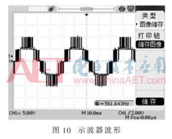
The oscilloscope displays the waveform as shown in Figure 10. Comparing Figure 10 with Figure 6, it can be seen that the oscilloscope waveform is completely consistent with the simulation results.
6 Conclusion
Aiming at the problem that the typical hybrid system working in high frequency state--the intelligent control and fault diagnosis DSP code of the inverter system has a long development cycle, low efficiency and cumbersome implementation, a method based on code generation technology is proposed. The code generation technology and its development flow are introduced. The three-level PWM code generation is taken as an example to expand the description. Finally, the three-level PWM code is debugged in the inverter physical system. The result proves that the method is simple and practical, the development cycle is short, the error rate is low, and the efficiency is obviously improved. It provides convenience for inverter intelligent control and fault detection and diagnosis algorithm practice verification, and has high practical value.
Cell Phone Case, Mobile Phone Covers, Clear Phone Case, Mobile Phone Case, TPU Phone Case, Silicone Phone Case
Shenzhen Jianjiantong Technology Co., Ltd. , https://www.jjtbackskin.com