Abstract: A design example for a portable data acquisiTIon system is offered that greatly simplifies the circuit design task. A reducTIon from seven components down to three components is accomplished with a design that has lower system cost, faster TIme-to-market, smaller size , better performance, and higher reliability.
The hardware design of a portable measurement system is more complicated than just choosing the right IC to meet the required electrical performance. There are many tradeoffs to be considered. Are there size constraints with board area or height? What does the total system cost, including the components, assembly, and final test, need to be? How important is TIme-to-market and have all the associated risks been identified? What is the product life cycle? In what environment will the product be used and what are the reliability requirements? At one extreme is a discrete design using readily available standard components and at the other extreme is a custom design using a single mixed-signal chip. The following will compare a discrete design to a design using the MAX1407.
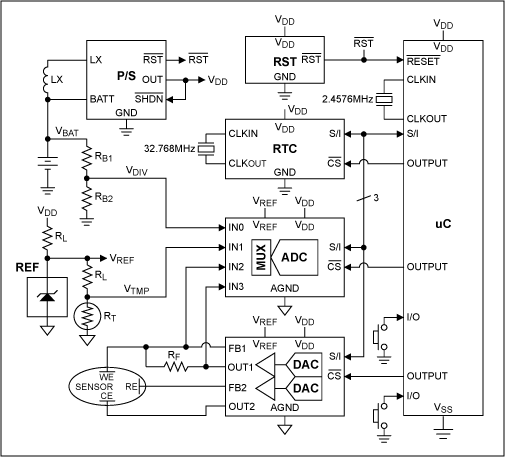
Figure 1 shows the functional block diagram for a portable data acquisition system (DAS) using discrete components. The system includes power, analog, and digital circuitry. The power is derived from the batteries, with a power supply for a regulated output voltage. The battery voltage can be measured on demand with the A / D converter and there are reset circuits for the battery and the regulated output voltage. The analog includes the analog front end (AFE) circuitry (which may include D / A converters, opamps, and analog switches) to interface with an electrochemical sensor, a thermistor circuit to measure temperature, an A / D converter with an input multiplexer, and a voltage reference for use with the AFE, thermistor, and A / D converter. The digital circuitry includes a 32kHz oscillator, real-time clock (RTC), and a microcontroller (µC) including a high-frequency crystal, external interrupts for the user interface, internal memory, and possibly other peripherals, such as a liquid cryst al display (LCD) bias and driver circuit to interface to an LCD.

Figure 1. Portable system functional block diagram with discrete standard components.
The sensor shown in Figure 1 is an electrochemical type sensor configured in a counter configuration where the working electrode (WE) is biased via the FB1 pin. The external resistor between FB1 and OUT1 configures the force / sense D / A converter as a transimpedance amplifier to measure the current through the sensor. The reference electrode (RE) is biased via the FB2 pin, and the feedback loop is closed through the sensor impedance to the OUT2 pin to regulate a constant potential between WE and RE over varying sensor currents.
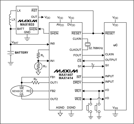
Figure 2 shows the functional block diagram for the same portable DAS using the MAX1407, simplifying the system design greatly. The MAX1407 contains all the circuitry required for the AFE, including the multiplexer, the A / D converter, and the voltage reference. It also has the ability to measure the battery and supply voltages. Also included are digital functions, including two reset circuits, a 32kHz oscillator with RTC, wake-up circuitry, power supply control, and a high-frequency clock output to drive the µC. In addition, all the blocks in the MAX1407 can be individually controlled and powered down via the serial interface. The sensor application shown is just one of the many ways this flexible AFE can be configured.

Figure 2. Portable system functional block diagram using the MAX1407 / 14.
There are many benefits with using the MAX1407 (or with similar devices, such as the MAX1408, MAX1409, or MAX1414, if the system requirements are different). These are lower system cost, faster time-to-market, smaller size, better performance , and higher reliability. See Table 1.
Table 1. MAX1407 / MAX1408 / MAX1409 / MAX1414 Selector Table
The system cost is lower for many reasons. There are far fewer components, resulting in a lower component cost using competitively priced MAX1407. The assembly and final test cost will be much lower because the total insertion cost is lower due to fewer components, and there is much less to test and verify at the board level. Also, the features included within the MAX1407 eliminate some functionality in the µC, such as the RTC, reset, and A / D converter, resulting in a greater selection of lower cost µCs from which to choose.
The time-to-market is faster because the analog design and a large part of the system design has been incorporated in the MAX1407. The board design and debug time will be faster because there are less components to manage. Once the first design has been completed, it will be very easy to spin-off new designs as long as the analog measurement system doesn't change significantly. If the changes are in the user interface, software features, memory requirements, or display then it is fairly simple to change the software or select another µC in the same family to provide a product variation or improved feature in a very short time.
The system size should be smaller and easier to fit into the required form factor because there are far less components and traces to route on the printed circuit board. The performance should be better than a discrete design because the functional blocks have been optimized to operate as a data acquisition system that will connect seamlessly to a µC and a power supply, if necessary without any additional circuitry. The reliability is also improved due to fewer components.
The MAX1407 / 08/09/14 family combines all of the analog and system support circuitry required by a portable or non-portable data acquisition system and connects seamlessly to an inexpensive, standard µC. Table 2 shows a comparison of the two design paths and quantitatively rates six important items to consider when embarking on a system design. The MAX1407 provides a superior solution to a discrete design when all these metrics are considered together.
Table 2. Comparison of Two System Design Paths
The hardware design of a portable measurement system is more complicated than just choosing the right IC to meet the required electrical performance. There are many tradeoffs to be considered. Are there size constraints with board area or height? What does the total system cost, including the components, assembly, and final test, need to be? How important is TIme-to-market and have all the associated risks been identified? What is the product life cycle? In what environment will the product be used and what are the reliability requirements? At one extreme is a discrete design using readily available standard components and at the other extreme is a custom design using a single mixed-signal chip. The following will compare a discrete design to a design using the MAX1407.
Figure 1 shows the functional block diagram for a portable data acquisition system (DAS) using discrete components. The system includes power, analog, and digital circuitry. The power is derived from the batteries, with a power supply for a regulated output voltage. The battery voltage can be measured on demand with the A / D converter and there are reset circuits for the battery and the regulated output voltage. The analog includes the analog front end (AFE) circuitry (which may include D / A converters, opamps, and analog switches) to interface with an electrochemical sensor, a thermistor circuit to measure temperature, an A / D converter with an input multiplexer, and a voltage reference for use with the AFE, thermistor, and A / D converter. The digital circuitry includes a 32kHz oscillator, real-time clock (RTC), and a microcontroller (µC) including a high-frequency crystal, external interrupts for the user interface, internal memory, and possibly other peripherals, such as a liquid cryst al display (LCD) bias and driver circuit to interface to an LCD.

Figure 1. Portable system functional block diagram with discrete standard components.
The sensor shown in Figure 1 is an electrochemical type sensor configured in a counter configuration where the working electrode (WE) is biased via the FB1 pin. The external resistor between FB1 and OUT1 configures the force / sense D / A converter as a transimpedance amplifier to measure the current through the sensor. The reference electrode (RE) is biased via the FB2 pin, and the feedback loop is closed through the sensor impedance to the OUT2 pin to regulate a constant potential between WE and RE over varying sensor currents.
Figure 2 shows the functional block diagram for the same portable DAS using the MAX1407, simplifying the system design greatly. The MAX1407 contains all the circuitry required for the AFE, including the multiplexer, the A / D converter, and the voltage reference. It also has the ability to measure the battery and supply voltages. Also included are digital functions, including two reset circuits, a 32kHz oscillator with RTC, wake-up circuitry, power supply control, and a high-frequency clock output to drive the µC. In addition, all the blocks in the MAX1407 can be individually controlled and powered down via the serial interface. The sensor application shown is just one of the many ways this flexible AFE can be configured.

Figure 2. Portable system functional block diagram using the MAX1407 / 14.
There are many benefits with using the MAX1407 (or with similar devices, such as the MAX1408, MAX1409, or MAX1414, if the system requirements are different). These are lower system cost, faster time-to-market, smaller size, better performance , and higher reliability. See Table 1.
Table 1. MAX1407 / MAX1408 / MAX1409 / MAX1414 Selector Table
Part Number | Total ADC Analog Inputs | ADC Auxilary Analog Inputs | ADC Data Ready Interrupt Signal | Differential Input Detection Threshold (mV) | Force / Sense DACs | External Power Supply Control | 3-State Digital Output |
MAX1407 | 8 DIFF | 4 | Yes | 0 | 2 | Yes | Yes |
MAX1408 | 8 DIFF | 8 | Yes | 0 | 0 | Yes | Yes |
MAX1409 | 4 DIFF | 1 | No | 0 | 1 | No | No |
MAX1414 | 8 DIFF | 4 | Yes | 50 | 2 | Yes | Yes |
The system cost is lower for many reasons. There are far fewer components, resulting in a lower component cost using competitively priced MAX1407. The assembly and final test cost will be much lower because the total insertion cost is lower due to fewer components, and there is much less to test and verify at the board level. Also, the features included within the MAX1407 eliminate some functionality in the µC, such as the RTC, reset, and A / D converter, resulting in a greater selection of lower cost µCs from which to choose.
The time-to-market is faster because the analog design and a large part of the system design has been incorporated in the MAX1407. The board design and debug time will be faster because there are less components to manage. Once the first design has been completed, it will be very easy to spin-off new designs as long as the analog measurement system doesn't change significantly. If the changes are in the user interface, software features, memory requirements, or display then it is fairly simple to change the software or select another µC in the same family to provide a product variation or improved feature in a very short time.
The system size should be smaller and easier to fit into the required form factor because there are far less components and traces to route on the printed circuit board. The performance should be better than a discrete design because the functional blocks have been optimized to operate as a data acquisition system that will connect seamlessly to a µC and a power supply, if necessary without any additional circuitry. The reliability is also improved due to fewer components.
The MAX1407 / 08/09/14 family combines all of the analog and system support circuitry required by a portable or non-portable data acquisition system and connects seamlessly to an inexpensive, standard µC. Table 2 shows a comparison of the two design paths and quantitatively rates six important items to consider when embarking on a system design. The MAX1407 provides a superior solution to a discrete design when all these metrics are considered together.
Table 2. Comparison of Two System Design Paths
Metric | MAX1407 (2-3 IC's) | DISCRETE (6-12 IC's) |
| Analog Performance | *** | ** |
| Reliability | *** | * |
| Small Size | *** | * |
| Time to Market | *** | ** |
| Ease of Spin-offs | *** | ** |
| System Cost | *** | * |
| Overall Rating | *** | ** |
Win 3 Unit Cap Lamp Charger CH01 is a smart charger that specially designed for Win3 Cap Lamps.
With Termoelectrical Protection System, and overcharging monitoring, it is Compatible with all our Win 3 Cap Lamps.
It can be mounted to the wall or the place convenient
Easy Manteinance and spare parts replacement.
Compatible with all our win3 cap lamps.
Wall Mount Qi Charger,Wall Mount Phone Charger,Wall Mounted Wireless Charger,Wall Mounted Wireless Phone Charger
ZHEJIANG HUACAI OPTIC-TECHNOLOGY CO LTD , https://www.win3safety.com