This paper introduces the single-chip solution of the SOC chip CSU8RP3119 used in the core power technology products. By using the chip's two high-speed PWM (16M) and four high-performance ADCs (12bit, deadband less than 3mV) and unique reference source digital correction patent technology, CSU8RP3119 can achieve up to 93% efficiency without the need for other peripheral ICs. Synchronous rectified mobile power, the efficiency is still higher than 88% under 2.1A output conditions.
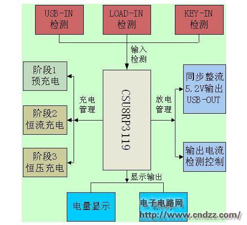
First, the system design mobile power consists of charge management, power management, input detection, display output (see the figure below). 
Second, the detailed design
2.1 PWM Controlled Charge Management (Alternative Charge Management Chip [TP4056/5056])
According to the chemical characteristics of lithium-ion batteries, the charging process can be divided into three stages: pre-charging, constant-current charging, and constant-voltage charging. The CSU8RP3119 can control the current and voltage of the charging process flexibly through the PWM controlled Bulk DC-DC circuit to meet the charging current and voltage requirements of different types of batteries, which fully guarantees the safety and effectiveness of the charging process.
2.2 PWM control power management (synchronous rectification can be implemented to replace the peripheral DC-DC chip)
Utilizing the CSU8RP3119's own high-speed PWM clock and subtly multiplexing the inductors and switching components used in the charging process, the synchronously rectified Boost DC-DC can achieve up to 95% discharge efficiency, taking into account the parasitic resistance of the mobile power system loop. The overall discharge efficiency can reach 93%, and the efficiency can still exceed 88% even under the condition that the discharge current reaches 2.1A.
2.3 Calibrate the internal 1.4V reference source with digital correction technique (eliminate external reference source [TL431 or HT7533])
The built-in 1.4V reference voltage of the CSU8RP3119 is inherently biased. By using a patented digital correction technique, the corrected error is less than 1%.
2.4. Mobile power battery security
The CSU8RP3119 provides a hardware-level protection mechanism for short-circuit and over-current of the battery. When the external power supply is short-circuited, the power monitoring circuit of the chip automatically turns off all output channels after the battery voltage is lower than 2V to ensure battery safety. In order to prevent the battery from being overcharged (for example, a 4.2V battery with a charging voltage exceeding 4.3V), the CSU8RP3119 uses a battery voltage directly as Vref, which in turn tests the internal 1.4V reference voltage, eliminating the need for an external voltage divider resistor. , thus avoiding the possibility of misdetection due to external circuit failure. The battery safety during the charging process is guaranteed. In addition, the feedback mechanism of the loop will be detected before the system is started and during the charging and discharging process, thus ensuring that the system operates under closed loop and safe conditions.
With the above multiple protection mechanism of hardware and software, if the lithium ion battery protection chip (such as DW01) is still used on the PCB, it can ensure that the protection mechanism of the lithium ion battery protection chip is not triggered, and thus does not need to be reactivated.
2.5 Safety of the charged device When the charged device is in a high current charging state (1A or 2.1A), if the charging socket is in poor contact, voltage overshoot may occur, thereby damaging the charged device, especially the software level. DC-DC. The maximum command speed of the CSU8RP3119 can reach 8M. After the time of one main cycle is optimized, it can be controlled within 200uS, thus effectively controlling the overshoot voltage. After testing, under 1A condition, the overshoot voltage does not exceed 6.0V, and the duration does not exceed 5mS. Under 2A conditions, the overshoot voltage does not exceed 6.3V and the duration does not exceed 5mS, which fully meets the safety requirements of charged devices such as mobile phones.
Description of Stacked D-Sub I/O Connectors
Antenk's connectors are designed for applications requiring multiple connector ports with limited PCB space
The condensed footprint of Antenk's dual port D-sub solution is available in four industry sizes, three connector spacing options, and six hardware configurations for one of the broadest stacked D-sub offerings on the market in standard and high-density variations.
Stacked D-sub I/O connectors are designed for applications requiring multiple connector ports with limited PCB space. Two right angle D-sub connectors are stacked one on top of another, creating a single dual-port connector with a very condensed footprint.
Features of Stacked D-Sub I/O Connectors
Available in four industry standard sizes:
Standard density: 9, 15, 25, 37
Available in three connector spacing options: 0.625", 0.750", 0.900"
Available in six hardware configurations
High-temperature UL94 V-0 thermoplastic (260°C process temp)
High performance stamped contacts
Applications of Stacked D-Sub I/O Connectors
Communications
Instrumentation
Medical
Computers/peripherals
Commercial industry
Test labs
Gaming industry
Range of of Stacked D-Sub I/O Connectors
Male Stacked D sub Connector
Female Stacked D sub ConnectorStandard Density Stacked D sub Connector
High Density Stacked D sub Connector
Dual-Port Stacked D-Sub Connectors
Dual Port (Stacked) D Sub,,Stacked D Sub I/O Connectors,Dual-Port Stacked D-Sub Connectors,Male Stacked D sub Connector, Female Stacked D sub Connector, Standard Stacked D sub Connector, High Density Stacked D sub Connector
ShenZhen Antenk Electronics Co,Ltd , https://www.antenkwire.com