Adopt TMS320F28335 to compose an application system, first consider whether the various functions of TMS320F28335 meet the requirements of the application system. If it can be satisfied, the system is the smallest application system. A minimum application system includes: reset circuit, clock circuit, power supply and memory, etc. For TMS320F28335, it has on-chip Flash, OTPROM and SARAM memory, and there is no need to consider external memory interface issues when designing the smallest application system.
The following is a connection method of F28335 minimum application system:

First introduce the MAX811 chip, the MAX811 chip guarantees the normal reset of the DSP chip.
VCC: Power
GND: DC ground
/RST: Auto-reset terminal (power-on reset terminal), active at low level. It is valid when the VCC voltage is lower than the reset threshold, and remains low for at least 140ms after the VCC voltage rises above the reset threshold.
/MR: Manual reset terminal, active low. It is valid as long as /MR is low, and the state of the reset pin will remain until 140ms after /MR returns to high.
Through the above explanation, it is easy to understand how the above reset circuit works.
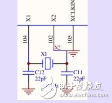
2. Clock circuit design

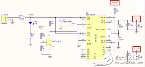
What used here is TPS767D301 power chip two-way power output to supply power for DSP chip and peripheral equipment. The system core voltage is 1.9V and the I/O port supply voltage is 3.3V.
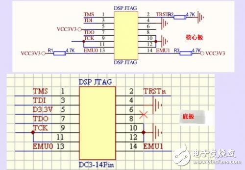
4. JTAG interface circuit
TMS320F28335 has an on-chip scan simulation interface (JTAG) that complies with the IEEE1149.1 standard, which is directly accessed through the emulator. In order to communicate with the emulator, the smallest system board designed should have a 14-pin emulation interface. The EMU0 and EMU1 signals must be connected to the power supply through a pull-up resistor, and the pull-up resistor is 4.7kΩ.
summary:The design circuit of the minimum application system of TMS320F28335 is given above, and the circuit is used to simulate and develop the TMS320F28335 system online in real time. However, this system is only a minimal application system, and the application system of specific modules should be designed according to actual needs.
Precautions:(1) The clock circuit adopts an internal crystal oscillator, which should be placed as close as possible to the TMS320F28335 when the circuit is configured, the lead should be short and thick, the capacitance should be stable, the capacitance value should be accurate, and it should be far away from the heating element.
(2) Use protective capacitors at the output of the power module, whose value cannot be less than 10μF, and cannot use chip capacitors or high-frequency ceramic capacitors, otherwise the work is unstable.
What used here is TPS767D301 power chip two-way power output to supply power for DSP chip and peripheral equipment. The system core voltage is 1.9V and the I/O port supply voltage is 3.3V.
Spring-type terminals are new types of spring-type terminals, which have been widely used in the world's electrical and electronic engineering industries: lighting, elevator control, instrumentation, power, chemistry, and automotive power.
If the terminal block is black, one of the possibilities is not necessarily burning black, oxidation may also be black. So how to verify whether it is burnt black? The method we take is to wipe it with a finger. If it can be wiped off, like soot, it is the black substance formed by oxidation, which can only be ground off with sandpaper or a file.
Spring Terminal,Spring Push-In Terminal Block,Spring Clamp Terminal Block,Spring Terminal Block For Pcb
Sichuan Xinlian electronic science and technology Company , https://www.sztmlchs.com