In a sonar system, it is necessary to digitize the acoustic signal input from the outside world for processing and analysis. The data acquisition module is responsible for the collection and transmission of analog signals. It plays a crucial role in the system, and the accuracy of the digitization has an important influence on the precision of later data processing. This paper uses 24-bit ∑-△ A / D data converter to build a 24-channel high-precision data acquisition module to meet the accuracy requirements of the sonar system on the data acquisition module and the number of acquisition channels.
1 hardware structure of data acquisition module1.1 Block Diagram of Data Acquisition Module
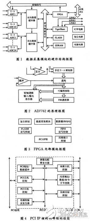
Figure 1 shows the hardware block diagram of the data acquisition module in this paper. It consists of 24 ∑-ΔA/D data converters, bidirectional data buffers, FPGA, TIgerSharc DSP, FLASH, SDRAM, clock circuit, reset circuit and power circuit. The composition consists of a ∑-ΔA/D data converter responsible for the acquisition and conversion of analog signals, an FPGA responsible for data acquisition control and data buffering for the entire module, and TIgerSharc DSPs responsible for the coordination of the entire module and the preprocessing of the converted data. The ∑-△A/D data converter and FPGA are introduced below.

1.2 Introduction to AD7762
The sigma-delta A/D converter used in this article is Analog Devices' AD7762 24-bit high precision data converter. Figure 2 shows its block diagram. It has the following features: Fully differential modulator input, on-chip differential amplifier for signal buffering, programmable oversampling rate, low-pass FIR filter with default or user-programmable coefficients, and synchronous input between multiple devices Pin. In the actual circuit PCB design, because the AD7762 is a noise-sensitive analog device, so in the specific PCB design needs to do the following aspects: A / D analog power supply alone, analog ground and digital ground, single point, differential The input line is equal in length and the impedance is equal to 100 Ω using a precise reference voltage source.
1.3 Acquisition Control Logic Principle and FPGA Implementation
FPGA mainly realizes the function of data acquisition control, data buffering and PCI bus controller of the whole module. In this article, FPGA adopts Cyclone II series EP2C20 chip of Altera Company, among them PCI bus controller adopts PCI IP kernel to design, simplify the development difficulty of PCI controller. Figure 3 shows the block diagram of the internal FPGA module. The following describes the design of the PCI IP core and its local interface control, data acquisition module, and data buffer FIFO.
1.3.1 PCI IP Core and Its Local Interface Control
This article uses Altera's PCI IP core to implement the hardware implementation of the PCI bus protocol. Figure 4 is a block diagram of the internal structure of the PCI IP core. In the specific design, the MegaWizard is used to instantiate the PCI IP core, and corresponding local interface control logic is needed to implement the connection between the DSP and the PCI IP core.

1.3.2 Data Acquisition Module
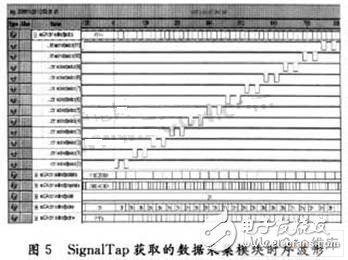
The data acquisition module completes the A/D initialization control and A/D data read control, in which the A/D initialization control completes the write operation to the A/D internal control register, and the A/D data read control completes the normal to the A/D data. Read. The specific control logic is designed according to the timing diagram of the AD7762. Figure 5 shows the timing waveforms of the data acquisition module acquired with the SignalTap in the Quartus II software.
1.3.3 Data Buffer FIFO
In order to solve the mismatch problem between the front-end data acquisition and the back-end data transmission, a data buffer FIFO is set inside the FPGA and the size is 4 kΩ/TImes; 32 b, the A/D converted data is directly stored in the FIFO, and the DSP The reading of the data in the FIFO is done by means of interrupts. The data buffer FIFO is instantiated through the MegaWizard. Only a small amount of read/write control logic is needed to make the FIFO work normally, and the size of the FIFO can be set flexibly within the range of RAM bits provided by the FPGA.
2 Data Acquisition Module ProgrammingAfter the module is powered on, the FPGA loads the configuration data from the EPROM and switches to the user state after initialization. The TIgerSharc DSP loads the program through the host and the program starts to run. After the A/D completes the initialization and synchronization, it is automatically collected. Data is written into the FPGA's internal FIFO. The DSP waits for the FIFO half-full interrupt signal to be generated. When the DSP detects the interrupt, it enters the corresponding interrupt service routine, reads the FIFO data into the on-chip memory of the DSP, and the DSP passes the data through the LINK interface. It is transmitted to the subsequent signal processing module. In addition, the data can be stored directly on the SDRAM on the data acquisition module. After the DSP performs some preprocessing, the data is transmitted to the subsequent signal processing module.
3 ConclusionThe 24-channel data acquisition module designed in this paper uses FPGA to implement functions such as data acquisition control, data buffering, and PCI bus controller, which simplifies the circuit, improves the reliability and stability of the module, and facilitates the functional upgrade of the module; The A/D data converter satisfies the sonar system's requirements for data acquisition accuracy; in addition, the Tiger-Sharc DSP also provides corresponding processing capabilities for data preprocessing. Therefore, the data acquisition module in this paper has a good engineering value and a wide range of application prospects.
Plywood Subwoofer,Plywood for Speaker Box,12 inch Plywood Subwoofer,8 inch Plywood Subwoofer
NINGBO LOUD&CLEAR ELECTRONICS CO.,LIMITED , https://www.loudclearaudio.com