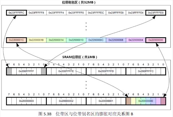
After a bit-band operation is supported, a single bit can be read or written using normal load/store instructions. In CM3, bit bands are implemented in two areas. One is the lowest 1MB range of the SRAM area, and the second is the lowest 1MB range of the on-chip peripheral area. The addresses in these two areas can be used in addition to the normal RAM. They also have their own "bit-band alias area". The bit-band alias area expands each bit into a 32-bit word. When you access these words through a bit aliased area, you can access the original bits.
The concept of a bit-band operation actually existed 30 years ago. It was a precursor to the 8051 microcontroller. Today, CM3 has evolved this capability. The bit-band operation here is a greatly enhanced version of the 8051-bit addressing area.
CM3 uses the following terms to denote the relevant address stored in the bit band:
Bitband: Address area with bit-band operation
Bit-band alias: Access to the alias address eventually applies to the bit-band access (this has an address-mapping process in the middle)
In the bit-band region, each bit is mapped to one word in the alias address area - this is the only word for which the LSB is valid. When an alias address is accessed, the address is first converted to a bit address.
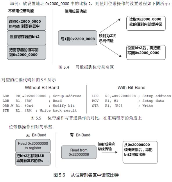
For read operations, read one of the bits in the bit-band address, move the desired bit right to the LSB, and return the LSB. For a write operation, the bit to be written is left shifted to the corresponding bit number, and then an atomic "read-modify-write" process is performed.


The range of two memory areas supporting bit-band operation is:
0x2000_0000â€0x200F_FFFF (minimum 1 MB in SRAM area)
0x4000_0000â€0x400F_FFFF (minimum 1 MB in on-chip peripheral area)
For a bit in the SRAM bit-band area, note that the byte address is A, and the bit number is n (0<=n<=7). The address of the bit in the alias area is:
AliasAddr=0x22000000+((A-0x20000000)*8+n)*4=0x22000000+(A-0x20000000)*32+n*4
For a bit in the on-chip peripheral bitband, note that the address of the byte where it is located is A, and the bit number is n (0<=n<=7), then the address of the bit in the alias area is:
AliasAddr=0x42000000+((A-0x40000000)*8+n)*4=0x42000000+(A-0x40000000)*32+n*4
In the above formula, "*4" indicates that one word is 4 bytes, and "*8" indicates that there are 8 bits in one byte.
Here's no more an example:
1. Write 0x3355AACC at address 0x20000000
2. Read address 0x22000008. This read access will read 0x20000000 and extract bit 2 with a value of 1.
3. Write 0 to address 0x22000008. This operation will be mapped to a "read-modify-write" operation (atomic) for address 0x20000000, clearing bit 2 to 0.
4. Now reading 0x20000000 will return 0x3355AAC8 (bit[2] is cleared).
Bits with aliased words are only LSBs meaningful. In addition, when the access bit has an aliased area, no matter which length of the data transfer instruction (word/halfword/byte) is used, the address is aligned to the word boundary, otherwise unpredictable results will be generated.
[cpp] view plain copy///////////////////////////////////////////////// ///////////////////
/ / Band operation to achieve 51 similar GPIO control function
/ / Concrete realization of the idea, reference <> Chapter 5 (pages 87 ~ 92).
//IO operation macro definition
#define BITBAND(addr, bitnum) ((addr & 0xF0000000)+0x2000000+((addr & 0xFFFFF)<<5)+(bitnum<<2))
#define MEM_ADDR(addr) *((volatile unsigned long *)(addr))
#define BIT_ADDR(addr, bitnum) MEM_ADDR(BITBAND(addr, bitnum))
//IO port address mapping
#define GPIOA_ODR_Addr (GPIOA_BASE+12) //0x4001080C
#define GPIOB_ODR_Addr (GPIOB_BASE+12) //0x40010C0C
#define GPIOC_ODR_Addr (GPIOC_BASE+12) //0x4001100C
#define GPIOD_ODR_Addr (GPIOD_BASE+12) //0x4001140C
#define GPIOE_ODR_Addr (GPIOE_BASE+12) //0x4001180C
#define GPIOF_ODR_Addr (GPIOF_BASE+12) //0x40011A0C
#define GPIOG_ODR_Addr (GPIOG_BASE+12) //0x40011E0C
#define GPIOA_IDR_Addr (GPIOA_BASE+8) //0x40010808
#define GPIOB_IDR_Addr (GPIOB_BASE+8) //0x40010C08
#define GPIOC_IDR_Addr (GPIOC_BASE+8) //0x40011008
#define GPIOD_IDR_Addr (GPIOD_BASE+8) //0x40011408
#define GPIOE_IDR_Addr (GPIOE_BASE+8) //0x40011808
#define GPIOF_IDR_Addr (GPIOF_BASE+8) //0x40011A08
#define GPIOG_IDR_Addr (GPIOG_BASE+8) //0x40011E08
/ / IO operation, only a single IO port!
//Ensure that the value of n is less than 16!
#define PAout(n) BIT_ADDR(GPIOA_ODR_Addr,n) //output
#define PAin(n) BIT_ADDR(GPIOA_IDR_Addr,n) //Enter
#define PBout(n) BIT_ADDR(GPIOB_ODR_Addr,n) //output
#define PBin(n) BIT_ADDR(GPIOB_IDR_Addr,n) //Enter
#define PCout(n) BIT_ADDR(GPIOC_ODR_Addr,n) //output
#define PCin(n) BIT_ADDR(GPIOC_IDR_Addr,n) //Enter
#define PDout(n) BIT_ADDR(GPIOD_ODR_Addr,n) //output
#define PDin(n) BIT_ADDR(GPIOD_IDR_Addr,n) //Enter
#define PEout(n) BIT_ADDR(GPIOE_ODR_Addr,n) //output
#define PEin(n) BIT_ADDR(GPIOE_IDR_Addr,n) //Enter
#define PFout(n) BIT_ADDR(GPIOF_ODR_Addr,n) //output
#define PFin(n) BIT_ADDR(GPIOF_IDR_Addr,n) //Enter
#define PGout(n) BIT_ADDR(GPIOG_ODR_Addr,n) //output
#define PGin(n) BIT_ADDR(GPIOG_IDR_Addr,n) //Enter
Lc Fiber Coupler,Lc To Sc Coupler,Sc To Lc Coupler,Mpo To Lc Adapter
Ningbo Fengwei Communication Technology Co., Ltd , https://www.fengweicommunication.com