This is Part 3 of a 3-part series: Part 1: Effects of Digital Crosstalk in Data Converters Part 2: Crosstalk on the Clock Crosstalk from digital data signals into the clock signal of a data-conversion system can cause hard-to-diagnose problems. This obscure problem is different than the crosstalk from digital data signals into the analog signal path, which was the subject of Part 1. There is value to understanding this different crosstalk problem at a deeper level, so a design engineer can more efficiently understand and troubleshoot a circuit with this type of problem. After reading this arTIcle, the reader will understand how harmonic distorTIon and other signal-dependant-error problems can be caused by crosstalk from digital data signals onto the clock.
Part 2 of this series covers basic principles that will help you understand the material in this arTIcle. Crosstalk from the Data Signals onto the ClockIn Part 2, we learned that noise that couples onto a clock signal looks sinusoidal and is at the same frequency as the input signal. With this understanding, it becomes clearer what happens in the frequency domain when there is crosstalk from the digital data signal onto the data converter clock. As analyzed in Part 1, the digital data signal from an ADC contains energy at the harmonics of the analog signal they sampled and represent. When the energy from this signal couples onto the data converter clock, it will have noise (in the form of jitter) at the harmonics of the analog signal. When this clock samples the subsequent analog signal, the analog signal will be effectively phase modulated at the rate of the same signal. This produces sidebands around the sampled signal at a distance of the frequency of the analog signal, which looks indistinguishable from harmonic distortion.
We will work through some example simulations of this for a simple sine wave. As seen in Part 1 of this article series, the digital bits have a pattern that is dependant on the input signal. For example, the MSB is a square wave at the input signal rate, as is shown in Figure 1.
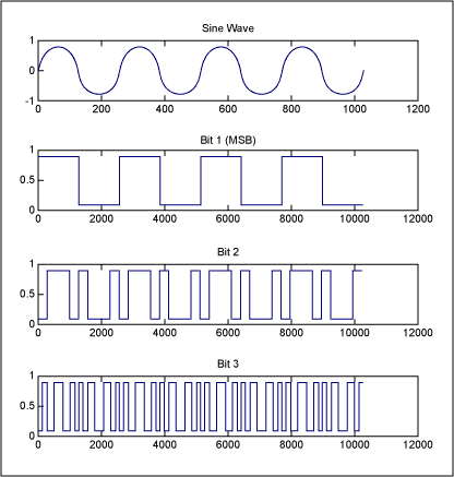
Figure 1. A sine wave at a frequency of 4 (cycles per sample set), and resulting digital bits.
We can look at these signals in the frequency domain. The easiest to understand is the MSB, which is a square wave at the same frequency as the analog signal. This MSB square wave has energy at the fundamental rate of the analog input signal and odd harmonics, as shown in Figure 2. Note that even harmonics would have shown up if there were any DC offset on the analog signal, which would have made the MSB approach more of an impulse than a 50% duty cycle square wave.
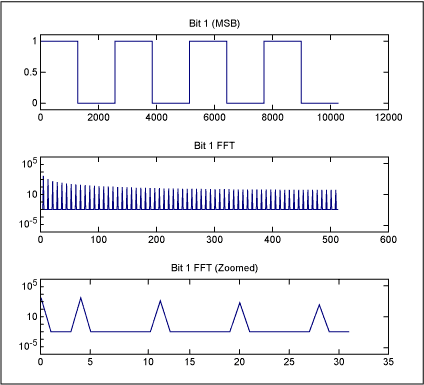
Figure 2. The MSB of a sine wave at a frequency of 4, and its frequency domain content:
When this bit couples through crosstalk onto the clock, altering the data converter sampling position, sidebands show up at a distance from the analog signal at the fundamental frequency, and odd harmonic frequencies, as shown in Figure 3. Note again that even harmonics would have shown up if there were a DC offset on the analog signal.
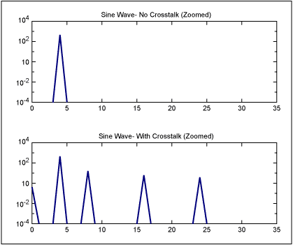
Figure 3. Pure sine wave at a frequency of 4, and the same sine wave with 1% crosstalk of the MSB onto the clock.
As another example, we will simulate a frequency of 5, for which the higher-order harmonic aliasing patterns do not land on the same frequencies as the fundamental and lower order harmonics. Figure 4 shows the frequency domain pattern of the MSB for a sine wave at a frequency of 5. Figure 5 shows the effect of this coupling via crosstalk onto the data converter clock signal. Note the same set of patterns is followed.
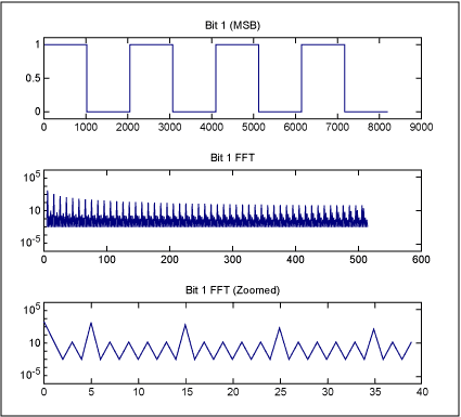
Figure 4. MSB of a sine wave at a frequency of 5, and its frequency domain content.
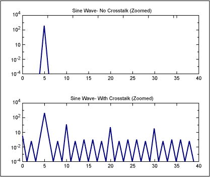
Figure 5. Pure sine wave at a frequency of 4, and the same sine wave with 1% crosstalk of the MSB onto the clock. Diagnosing and Solving the ProblemHere are some quick tips for dealing with noisy clocking problems. The biggest key is quickly diagnosing if your problem is caused by clock jitter or something else.
In Part 1 of this article series, we mentioned that the effect of clocking jitter is directly proportional to the slope of the analog signal with respect to time. You can take advantage of this to see if you have a jitter problem by performing tests at different frequencies and analog amplitude levels. In looking at different frequencies, a jitter problem often predictably creates an effect that will increase proportionately with frequency (ie, 2x the input frequency creates a 2x larger sideband). In contrast, while most harmonic distortion problems get worse with higher frequencies, few have the exactly proportional dependence that the jitter effect does. Likewise in the analog amplitude level variation, the jitter effect will keep the ratio between the signal and noise / distortion / sideband caused by the jitter equal irrespective of analog level ( an exception is if a lower analog signal creates lower bit activity which can reduce jitter which can reduce the noise). In contrast, analog harmonic distortion typically will decrease its ratiometric effect with decreasing input level.
As a practical tip in using the above phenomena to your advantage, run experiments with the highest possible analog frequency to exaggerate the effects. If your system allows it, increasing the input signal significantly beyond the Nyquist rate of the ADC is an acceptable, and very useful technique to exaggerate the effect.
Ideally, you could just measure the jitter on the clock with an oscilloscope or some instrument. However, most oscilloscopes don't have sufficient performance to see the low level jitter that can cause problems in most data converter systems. A common instrument that can be useful in seeing the noise on a clock is a spectrum analyzer. On a spectrum analyzer, the clock should only look like a fundamental and odd harmonics. Anything else is noise / jitter. If the clock can be at a flexible frequency, again, run it at the highest possible frequency. The reason is while the picoseconds of jitter on the clock is typically independent of the frequency of the clock, the sidebands that show up on the clock measured with a spectrum analyzer will be higher with a higher frequency clock with the same amount of picosecond jitter, which makes them easier to see.
A very useful technique for finding jitter problems in ADCs not caused by digital signal bit crosstalk is to set the analog input frequency to a harmonic of the same rate, which will alias the signal to DC. If there is jitter on the clock, the noise will remain.
To design around and / or fix these problems, a designer needs to take similar precautions with the clock signal as he would with an analog signal; keep it separate from other digital logic or anything else that could have other frequency content. Don't run the clock through an FPGA that has any activity in it. If it is within the design constraints, keep all clock circuitry on separate power supplies, or at least, very filtered and / or regulated power supplies. Sometimes it can be appropriate to put the clock circuitry on its own ground plane (however, awareness of return currents and their effects are necessary to effectively design using multiple ground planes). Using a differential clock can significantly help. ConclusionDigital crosstalk of bits on an analog signal can create jitter, which can create harmonic distortion or other noise effects that can be very difficult to distinguish from analog harmonic distortion or noise effects. However, being cognizant of the effects, how they m anifest themselves, and how they change under different conditions can help a designer plan a quick and effective debugging strategy to determine if crosstalk onto the data converter clock is the cause of the designer's problem.
Laptop Stand Gaming Rgb,Laptop Stand Gaming Laptop,Gaming Laptop Stand Adjustable Height,Gaming Laptop Stand With Cooling,etc.
Shenzhen Chengrong Technology Co.ltd is a high-quality enterprise specializing in metal stamping and CNC production for 12 years. The company mainly aims at the R&D, production and sales of Notebook Laptop Stands and Mobile Phone Stands. From the mold design and processing to machining and product surface oxidation, spraying treatment etc ,integration can fully meet the various processing needs of customers. Have a complete and scientific quality management system, strength and product quality are recognized and trusted by the industry, to meet changing economic and social needs .
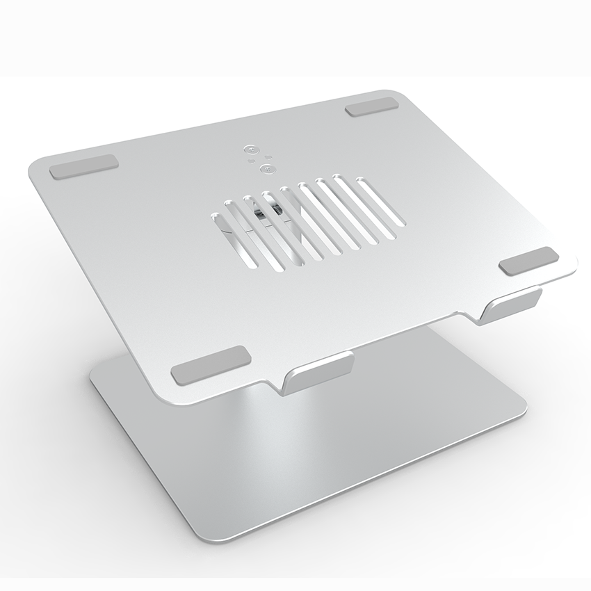
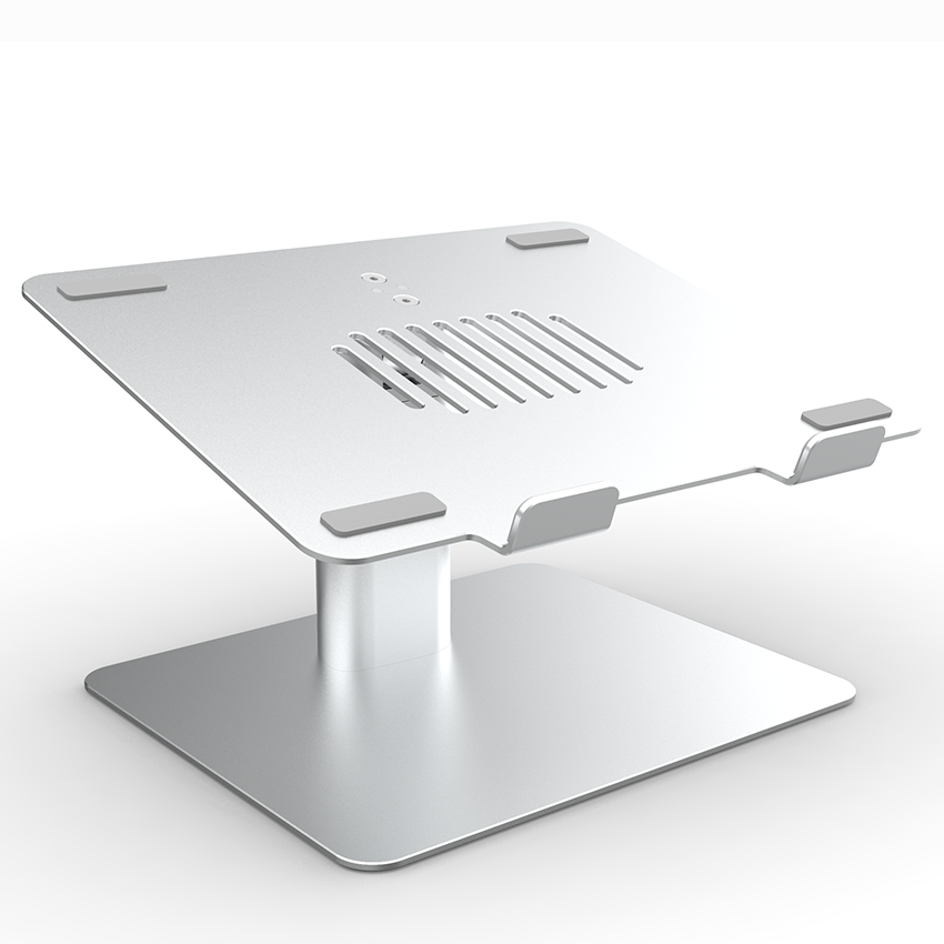
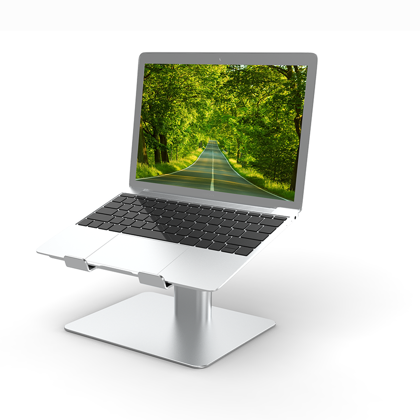
Laptop Stand Gaming Rgb,Laptop Stand Gaming Laptop,Gaming Laptop Stand Adjustable Height,Gaming Laptop Stand With Cooling
Shenzhen ChengRong Technology Co.,Ltd. , https://www.chengrongstand.com