PLD chips using this structure include: Altera's MAX7000, MAX3000 series (EEPROM process), Xilinx's XC9500 series (Flash process) and LatTIce, most of Cypress's products (EEPROM process)
Let's take a look at the overall structure of this PLD (take the MAX7000 as an example, the structure of other models is very similar to this):

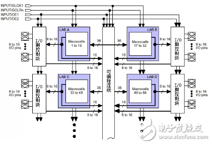
Figure 1 PLD internal structure based on product terms
This kind of PLD can be divided into three structures: Marocell, Programmable Line (PIA) and I/O Control Block. The macro unit is the basic structure of the PLD, which implements the basic logic functions. The blue part in Figure 1 is a collection of macrocells (because there are many macrocells, not drawn one by one). Programmable wiring is responsible for signal transmission, connecting all macrocells. The I/O control block is responsible for controlling the electrical characteristics of the input and output. For example, an open collector output, slew rate control, and three-state output can be set. Figure 1 Upper left INPUT/GCLK1,
INPUT/GCLRn, INPUT/OE1, INPUT/OE2 are global clocks, clear and output enable signals. These signals have dedicated connections to each macrocell in the PLD. The signal has the same delay to each macrocell. And the shortest delay.
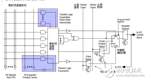
The specific structure of the macro unit is shown in the figure below:

Figure 2 Macro cell structure
On the left is an array of product terms. Actually it is an AND or array. Each intersection is a programmable fuse. If it is turned on, it implements AND logic. The latter product selection matrix is ​​an "or" array. Both combine logic together. On the right side of the figure is a programmable D flip-flop. Its clock and clear inputs can be programmed, dedicated global clear and global clocks can be used, and clocks generated by internal logic (product term arrays) can be used and cleared. . If a flip-flop is not required, this flip-flop can be bypassed and the signal is either output directly to the PIA or to the I/O pin.
Second, the product realization structure PLD logic realization principleHere we take a simple circuit as an example to specifically explain how the PLD uses the above structure to implement logic. The circuit is as follows:

image 3
Assume that the output of the combinational logic (the output of AND3) is f, then f=(A+B)*C*(!D)=A*C*! D + B*C*! D (We use !D to denote D's "not")
The PLD will implement the combinational logic f in the following way:

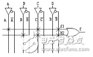
Figure 4
A, B, C, D enter the programmable connection array (PIA) after being input by the pin of the PLD chip. There will be A, A, B, B, C, C, D, and D in the internal. Output. Each fork in the figure represents a connection (programmable fuse is turned on), so we get: f = f1 + f2 = (A*C*!D) +
(B*C*!D). This combination of logic is achieved. The realization of the D flip-flop in the circuit of Fig. 3 is relatively simple, use the programmable D flip-flop in the macro unit to realize directly. The clock signal CLK is input by the I/O pin into the global clock dedicated channel inside the chip and is directly connected to the clock end of the programmable flip-flop. The output of the programmable flip-flop is connected to the I/O pin and the result is output to the chip pin. The PLD thus completes the function of the circuit shown in Figure 3. (The above steps are all completed automatically by the software and do not require human intervention.)
The circuit in Figure 3 is a very simple example and only needs one macro cell to complete. However, for a complicated circuit, a macro cell cannot be realized. At this time, multiple macro cells need to be connected through a parallel extension and a shared extension. The output of a macro cell can also be connected to a programmable line array. Input for another macrocell. This way PLDs can implement more complex logic.
This kind of product-based PLD is basically manufactured by EEPROM and Flash process, and it can work on power-on, without the need of other chips.
Silicone Keypad,Silicone Keyboard,Customized Rubber Keypad,Custom Silicone Keypad
CIXI MEMBRANE SWITCH FACTORY , https://www.cnjunma.com