Vision-based systems have become very common in many industries and applications. In fact, many of us carry an embedded vision system every day, such as in our smartphones. These smart devices not only capture images and record video, but also perform augmented reality applications, demonstrating how embedded vision technology is widely accepted.
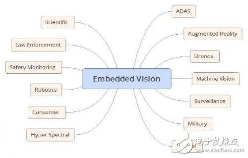
Increased processing power, memory density, and system integration have contributed to the growth of embedded vision in both traditional and emerging applications (examples shown in Figure 1). This also makes embedded vision widely accepted in the consumer, industry and government sectors and will achieve significant growth within a decade. Table 1 lists some of the high-growth areas of embedded vision, some of which are obvious and some of which are not obvious.

Figure 1 Common embedded vision applications.

Table 1 Expected embedded visual high growth areas
What is embedded vision?The embedded vision system contains the entire signal chain that receives light from the selected imaging sensor to the system output. System output refers to processed or unprocessed images or information extracted from an image and provided to downstream systems. Of course, embedded system architects are responsible for ensuring end-to-end performance based on system requirements.
To this end, embedded vision system architects need to be familiar with the various concepts and technologies associated with sensors and aftertreatment systems. This article is intended as an advanced primer to give readers a basic understanding of these technologies and concepts.
First you need to be familiar with the electromagnetic spectrum and the spectral domain where you want the system to operate. The human eye can only see the spectrum between the wavelengths of 390 nm (blue light) and 700 nm (red light), which is commonly referred to as the visible spectrum; the imaging device can capture images of a wider wavelength, including the technology used, including X-ray, ultraviolet, infrared, and visible spectrum.
In the near-infrared spectrum and below, we can use a charge-coupled device (CCD) or CMOS [2] (complementary metal-oxide-semiconductor) image sensor (CIS); in the infrared spectral range, a dedicated infrared detector is required. The infrared spectrum range requires dedicated sensors, in part because of the excitation energy required by chip imagers such as CCD or CIS. These devices typically require 1 eV of photon energy to excite an electron. However, in the infrared range, the photon energy is between 1.7 eV and 1.24 meV, so the infrared imager should be based on HgCdTe or InSb. These devices require lower excitation energy and are often used in conjunction with CMOS readout ICs (ie, ROICs) to control and sense the sensor.
The two most common detector technologies are CCD and CIS• Charge-coupled devices are considered analog devices, so integrating them into a digital system requires the use of an off-chip ADC and clock generation at the desired analog voltage level. Each pixel stores a charge generated by a photon. In most cases, pixels are arranged in a 2D array to form multiple rows, each row containing multiple pixels. When the CCD is read out, each line is transferred in parallel to the read register by line transfer, and each line is serially read out through the read register. During this register readout, the charge is converted to a voltage.
CMOS imaging sensors enable tighter integration, allowing the ADC, bias, and driver circuitry to be integrated on the same die. This greatly reduces system integration requirements and increases the complexity of CIS design. At the heart of the CIS is an Active Pixel Sensor (APS), where each pixel contains both a photodiode and a sense amplifier, so unlike a CCD, CIS can read any pixel address in the array.
Although most embedded visions use CIS devices, CCDs are still used in high-end research applications where performance is critical. The main points of this paper apply to both imaging technologies.
Lithium Iron Phosphate Battery
FEATURES & BENEFITS
Saintish 12.8V Lithium Iron Phosphate Battery built-in BMS to protect it from overcharge/discharge, temperature and short circuit. Monitors the battery operation status on mobile devices in real time with the built-in Bluetooth module.
Grade A prismatic battery cells ensure a more than 3000 cycles lifespan, which is more than 10 times to Lead Acid with 200~500 cycles. Wide operating Temp: Charge: 0°C~45°C; Discharge: -20°C~60°C.
The portable lithium battery pack's case material is ABS-FR material and the enclosure protection is IP65 waterproof, which lets you free from worrying about installing batteries indoors or outdoors. LiFePO4 Battery supports series(Up to 4 pcs) and parallel(up to 4pcs) connections.
Lithium Iron Phosphate Battery, 12.8V Lithium Battery, Rechargeble Battery, Lithium Battery for Caravan
Hangzhou Saintish Technology Co.,Ltd. , https://www.saintishtech.com