The application of 5G technology will use a number of different frequency bands, and the allocation of 5G frequency bands in different countries also has different solutions. Among them, there are relatively low frequency bands (300 MHz to 30 GHz), and relatively high frequency bands, and also include millimeter wave bands (30 to 300 GHz). Based on past design experience, the difference in PA design between PAs (power amplifiers) operating at lower frequencies and those operating at relatively higher frequencies is not significant. However, the wireless communication network based on 5G technology is very different from the traditional cellular network system. When designing a power amplifier suitable for 5G technology, engineers have to deal with the problems of RF microwave and millimeter wave simultaneously.
There are significant differences in the factors that need to be considered when designing RF microwave circuits and designing millimeter-wave circuits. Moreover, the high frequency wiring boards required for microwave circuits are also very different from those required for millimeter wave applications. This article will point out which board is best suited for applications in the microwave or millimeter wave band power amplifiers.
In general, most 5G system applications do not operate at frequencies higher than 6 GHz. Moreover, the power levels of systems in these low frequency bands are also higher than those in the millimeter wave band. The performance of RF microwave 5G power amplifiers depends on many key characteristics of the circuit board, including good thermal management, low insertion loss, and uniformity of RF performance over a wide temperature range. It also includes a well-controlled dielectric constant (Dk or εr). ), high thermal conductivity, low TCDk (Dk thermal coefficient), low loss factor and tightly controlled media thickness.
Let's take a look at each of the properties of the material and why they are critical to the characteristics of the RF microwave power amplifier. Many 5G RF microwave power amplifiers use a Doherty structure. The circuit of this structure requires the design of a quarter-wavelength line as the impedance transformation. If the wavelength-dependent PCB material variables are well controlled, the performance of the quarter-wave line circuit can be achieved as expected. Variables associated with this include material Dk and media thickness. Variable factors in the PCB manufacturing process also affect the performance of the quarter-wave line circuit, such as wire accuracy and conductor thickness.
In general, high-frequency circuit boards with a Dk tolerance of ± 0.05 are considered to be good performance materials that can be used for such applications. In addition, the substrate dielectric thickness of the material should be controlled to ±10% or less.
Another RF microwave power amplifier design point is the impedance matching network, the purpose is to match the external impedance to the power amplifier tube input or output. Impedance control and wavelength are affected by the same variables. However, the effects of these variables on the two are different. Many engineers believe that the change in Dk is the main influencing factor in the impedance change. However, this is usually not the case. Using any impedance calculation software, you can perform a very simple calculation to see the level of influence of the different variables that affect the impedance change. The relevant results are shown in Table 1.

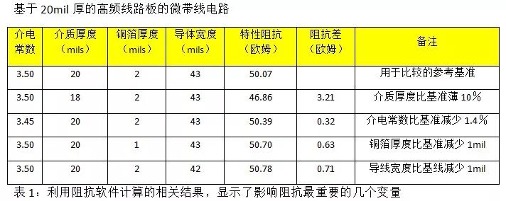
The data in Table 1 is based on a microstrip line circuit using a high frequency line sheet with a thickness of 20 mils, a nominal Dk of 3.50, and a Dk tolerance of ± 0.05. The first line of information is used as a reference or reference data, and the line shows that the obtained impedance value is 50.07 ohms. The other rows in Table 1 show the effect of changing one of the variables on the impedance. It can be seen that the most important factor in causing impedance changes is the dielectric thickness. After that, the control of the conductor width and the thickness of the copper foil changes the impedance value, and finally, Dk has the least influence on the change of the impedance value.
A further consideration when designing RF microwave power amplifiers is thermal management. Material thermal conductivity (or thermal conductivity) is a material property that can help reduce this problem. Most high frequency circuit boards have low thermal conductivity, typically between 0.2 W/m ∙K and 0.3 W/m ∙K. The value of the PCB material with a good thermal conductivity is considered to be 0.5 W/m/k or higher. The higher thermal conductivity allows heat to be transferred from the high-frequency circuit material of the power amplifier tube for better heat flow, allowing the circuit to dissipate heat more efficiently.
At the same time as heat conduction problems occur, many RF microwave power amplifiers are required to be used over a wide temperature range and to maintain normal operation. The dielectric constant temperature coefficient (TCDk) of a circuit board is the property of a material that describes the effect of temperature changes on the Dk value. As mentioned earlier, the change in Dk is not the biggest influence on the change of circuit impedance. However, the change of Dk will affect the wavelength, which will definitely cause problems in the performance of the quarter-wave line often used in Doherty power amplifiers. Based on experience, a good TCDk value should be |50| ppm/°C or lower, and an ideal TCDk value should be 0 ppm/°C, or the Dk value does not change with temperature. The graph of Figure 1 shows the TCDk characteristics of several different types of materials.
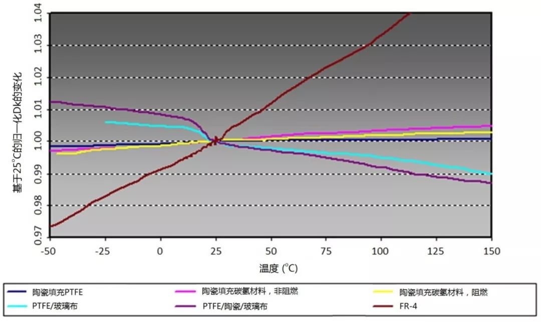
Figure 1: TCDk curves for different types of circuit boards
It can be seen that the dark purple curve indicates that the Tk/ceramic/glass cloth material has a very large change in Dk near room temperature, which is normal for polytetrafluoroethylene. If the polytetrafluoroethylene material is properly formulated, the Dk change caused by the influence of room temperature can be minimized or even eliminated, which is the case represented by the dark blue curve. This curve represents a ceramic-filled PTFE material, such as Rogers' RO3003TM laminate, which has a TCDk value of only -3 ppm/°C. The yellow curve represents a non-polytetrafluoroethylene thermoset that also has good TCDk characteristics of approximately 50 ppm/°C. This curve shows the variation of Rogers RO4350BTM (or RO4835TM) sheet.
The brown curve shows the FR-4 data and is shown as a reference in the chart. FR-4 is not a good TCDk material formulation, but it can be used as a counterexample to look at examples of materials with particularly poor TCDk properties. The ideal TCDk is a flat curve centered on 1.00 on the y-axis.
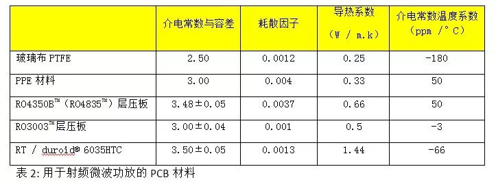
Finally, the material's dissipation factor (Df or Tanδ) also affects the thermal performance of many different circuit characteristics and circuits. Basically, circuits with low Df circuit boards will have lower insertion loss, while lower loss circuits will generate less heat. For RF microwave power amplifiers used in the frequency band below 6 GHz, the Df of the board used can basically meet the relevant requirements when the Df is below 0.005.
Table 2 summarizes the key material properties of the RF microwave power amplifier, which lists the different circuit boards and their parameters related to the performance of the amplifier, especially the reduction of heat generation.
The material considerations for 5G millimeter wave applications are similar to those in the RF microwave band; however, at higher frequencies, there are many other issues to consider. Especially in the millimeter wave band, the insertion loss becomes high, and at higher frequencies, the control of Dk and TCDk becomes more important as the wavelength decreases.
For PCBs in the RF section of millimeter-wave power amplifiers, thin, high-frequency plates with very low losses are often used. At millimeter wave frequencies, a thinner dielectric thickness helps to avoid spurious modes and resonances. In general, 10 mil thick dielectric materials can be used for 30 to 60 GHz applications, while 5 mil thick materials can be used at frequencies above 60 GHz. Of course, the above is just a summary of the experience, but there are exceptions.
The most commonly used RF structure for millimeter wave applications is the microstrip line and grounded coplanar waveguide (GCPW). When a microstrip line is used and there is impedance conversion, such as signal conversion from the RF connector to the circuit, GCPW is typically used for these transition regions, while the rest of the circuit is a microstrip line. Microstrip lines have some drawbacks, such as being more susceptible to radiation loss than GCPW, and having dispersion. In addition, there are few design methods for microstrip lines that can effectively suppress spurious patterns. If the GCPW structure is properly designed at a millimeter wave frequency, the radiation loss and dispersion effects can be greatly reduced or even eliminated. In comparison, the disadvantage of GCPW is that its RF performance is more susceptible to changes in related factors in PCB manufacturing [1], which may result in large variations in performance between different circuits even for the same GCPW design.
Since thin dielectric materials are required in the millimeter wave band, it is more complicated to reduce the insertion loss than in the RF/microwave band. For applications in the RF/microwave band, the signal wavelength is larger, the line plate is usually thicker, and the conductor-related insertion loss component—the conductor loss—is much smaller. For the millimeter wave band, the conductor loss, especially the surface roughness of the copper foil, will be an important factor affecting the insertion loss.
For example, for a thinner microstrip circuit, the so-called copper foil surface roughness refers to the roughness of the substrate-copper foil interface. When the skin depth is smaller than the roughness depth of the copper foil, the surface roughness of the copper foil has a significant effect on the conductor loss. [2] Figure 2 shows the difference in insertion loss of the surface roughness of different copper foils using microstrip lines of commonly used materials in millimeter wave applications.
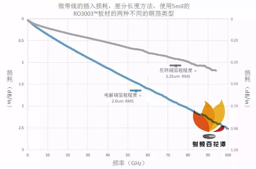
Figure 2: Comparison of the insertion loss of the microstrip line circuit using the same dielectric material, the surface roughness of the two different copper foils.
In addition, the rougher copper foil surface causes a decrease in phase velocity, which will make the circuit look as if it were on a higher Dk material. The following dielectric materials, different types of copper foil, are used to demonstrate this point through a simple experiment. There are significant differences in the surface roughness of copper foil for different copper foil types. The surface roughness of each copper foil was measured using a non-contact copper foil roughness tester before being fabricated into a laminate. After the laminate was fabricated, a 50 Ω microstrip transmission line circuit was fabricated on the laminate. Then the phase response test is performed on the circuit, and their effective Dk versus frequency is plotted, as shown in Figure 3.
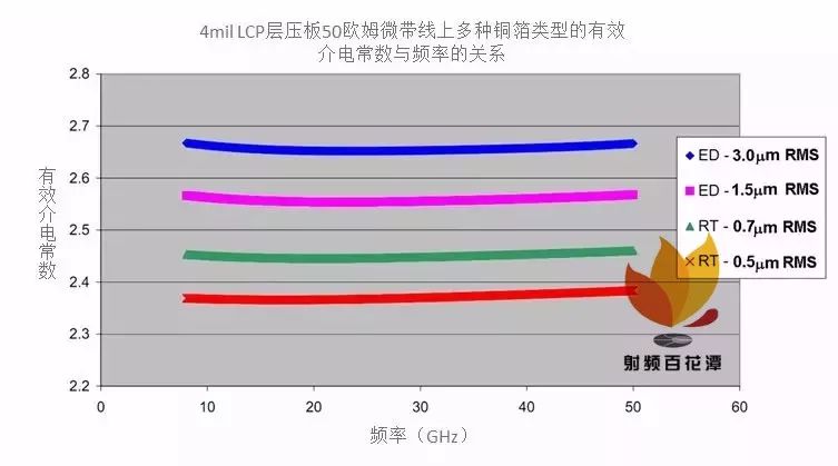
As can be seen in Figure 3, the circuit of the laminate using the smoothest copper foil on the surface (having an average surface roughness of 0.5 μm RMS, red curve) has the lowest effective dielectric constant. The trend in the figure is very obvious: the surface roughness increases and the effective Dk value increases. Basically, a rough copper foil causes a slower phase velocity, while a slower wave propagation is considered to have a higher dielectric constant. As can be seen from the figure, the effective Dk between the circuit of the smoothest copper foil and the circuit of the roughest copper foil differs by about 0.3. When considering that all circuits use the same medium, this is a very large difference for effective Dk, and it is the difference in surface roughness of the copper foil that leads to this large effective Dk difference.
As shown in Fig. 2, a similar test was performed on the difference in dielectric constant of the circuit due to the difference in surface roughness of the copper foil, and also a method of testing the phase response. Using the microstrip line phase response tool and the MWI-2018 tool software, a plot of Dk versus frequency can be obtained, as shown in Figure 4. The tool software can be downloaded free of charge at Rogers' technical support center. (Click "Read the original" at the end of the text to jump directly)
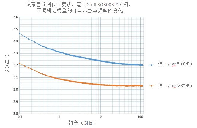
Figure 4: Microstrip line circuit Dk vs. frequency plot, testing copper foil using the same medium, different types and different surface roughness.
The Dk obtained in Figure 4 is the Dk or design Dk presented by the circuit. The inherent Dk of the high frequency line material medium used in the figure is 3.0. When the circuit is laminated with a rough copper foil, the wave propagation rate will slow down and Dk will increase. This is the case with circuits using ED copper. When the circuit uses a very smooth rolled copper, the phase velocity does not decrease significantly. Therefore, the Dk value is relatively low at this time and is close to the inherent Dk value of the medium. In theory, if the copper foil is completely smooth, the Dk curve will be close to 3.0, equal to the Dk value of the dielectric material.
The effect of a conductor on a thin circuit is much larger than that of a thicker circuit. If a thicker dielectric material is used for the same experiment as in Fig. 4, the obtained data curve will be different from the data in the original Fig. 4, and the difference in Dk test results obtained by the copper foil having different roughness will be reduced. When the circuit uses a 20 mil thick material, the smooth copper with a smooth surface has a Dk value of about 3.005 at 20 GHz, which is very close to the intrinsic Dk of a material having a value of 3.0; and the Dk value at 20 GHz using a rough surface ED copper. It is about 3.060 and the difference between the two is only about 0.055. Therefore, for thicker materials, the difference between the Dk values ​​is smaller because the thicker dielectric material does not receive larger conductors (ie, copper foil surface roughness) as in the thinner circuit shown in Figure 4. Impact.
Since the thinner circuit is more sensitive to the roughness of the conductor, ie the copper foil, the effect of considering the surface roughness of the copper depends not only on the overall insertion loss of the circuit, but also on the design Dk. In addition, the phase response of the circuit and the consistency of the design Dk also depend on the surface roughness of the copper foil. The surface roughness of the copper foil used to manufacture the high frequency laminate is normally changed. Variations in the surface roughness of the copper foil include variations with batch-to-batch and surface roughness along the board. However, the smoother the copper foil, the smaller the variation in the surface roughness of the copper foil. And because the surface roughness of the copper foil will affect the design Dk and phase response, the copper foil with smooth surface and small roughness variation will have more consistent circuit performance when performing different batch evaluations of the same circuit.
The world of wireless communication is rapidly evolving to the fifth generation of mobile communication (5G) technology, requiring the use of higher frequency millimeter wave bands. Power amplifiers and board materials for these power amplifiers are needed in these wireless networks, but choosing the best board for the circuit in the millimeter wave band requires more consideration than selecting the board for the RF/microwave band. . In summary, key features of materials used in RF/microwave power amplifiers include insertion loss, consistency of Dk, uniformity of dielectric thickness, thermal conductivity, and TCDk. These same material properties are equally suitable for millimeter-wave power amplifiers, except that the material will be thinner and more susceptible to the surface roughness of the copper foil.
60V20Ah Lithium Ion Battery,Waterproof Battery Pack For Bicycle,60V 20Ah L-Ion Waterproof Battery,Rechargeable 60V Lifepo4 Lithium Battery
Jiangsu Zhitai New Energy Technology Co.,Ltd , https://www.jszhitaienergy.com