This article shows two examples of the application of nanotechnology in microelectronics connections. Nanotechnology is a product that manipulates atoms and molecules in a spatial scale of 0.1 to 100 nm, processes materials, manufactures products with specific functions, or studies a substance to grasp the laws and characteristics of its atoms and molecules. New high technology.
This article refers to the address: http://
Nano printing technology
In the semiconductor industry, microfabrication technology is an indispensable technology for achieving integration and high performance of devices. However, when processing at a micron scale or lower, it is necessary to eliminate vibration in a cleaning environment, maintain a certain processing environment temperature, and suppress dimensional changes caused by thermal expansion, thereby increasing a considerable cost.
In recent years, in the United States, many countries have begun to use micro-joint printing, capillary micro-templates, dip-printing, etc. to easily form new nano-structured manufacturing technologies. This new processing technology is called flexible printing. Surgery. It differs from the development point of microfabrication technology in that its greatest feature is simplicity and low cost. Nanoprinting technology in flexible printing is simple in principle, and existing molding equipment is on the market.
1 nano printing technology
The basic principle of the nano-printing technique is shown in Fig. 1. The template having the nano-scale concave-convex pattern is extruded on the substrate coated with the resin film, and the concave-convex pattern is reproduced on the surface of the resin film. In the conventional nano-printing technology, the template can be copied at a constant magnification, and in the aspect ratio nano-printing technique, a structure higher than the concave portion of the nano-template can be formed.

Figure 1 Principle of nano printing
In the nanoprinting process, a resin film is first coated on a glass and a silicon substrate by a spin method or the like, and then the resin film is heated to be composited on the substrate. Then, the nano-template is extruded on the softened resin, and finally the nano-template is separated from the resin film. Through the above process, the pattern of the surface of the nano-template is copied on the surface of the resin film.
2 aspect ratio microstructure formation
In the nanoprinting technique, a metal punch is pressed onto a resin film to form a concave portion. However, in order to form a relatively large flat structure, it is necessary to have a deep-engraved nano-template. Since the template is detached from the resin film, the resin is inevitably stretched, so that a columnar structure higher than the concave portion of the nano-template can be formed. Known as the aspect ratio nano-printing technology.
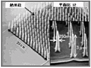
In the aspect ratio nano-printing technique, a nano-scale columnar structure aggregate having a diameter of 25 nm and a height of 3 μm (plane ratio of 12) can be simply formed (see Fig. 2). This structure is difficult to form in conventional precision plastic molding, but it can be molded by one-time rolling using an aspect ratio nano-printing technique.

Figure 2 Nano-pillar structure formed by nano-printing technology
3 prospects
Nano-printing technology is considered to be the closest to practical manufacturing technology, and nano-printing devices are already on the market in Japan. However, in order to form a good structure, it is necessary to develop a related technology that is guided by nano-templates and resin materials. Currently, this research is being carried out worldwide. The application of this technology will focus on the electronics sector, but it will also begin to involve areas such as edge energy.
Nano connection technology
The basic properties of nanoparticles (such as high durability, low melting point and low sintering temperature) are well known, but many of their applications have not been extended. Some people have proposed the use of nano-particle surface energy and low-temperature sintering function as a new solution for connecting materials. After the low temperature connection by the connection method, the sintered nanoparticles have a high melting point at the joint, which is very suitable for lead-free soldering which is difficult to connect at a high temperature. Here we mainly introduce the characteristics of the joint process of organic-silver composite nanoparticles and their applicability in electronic soldering.
1 Characteristics of organic-silver composite nanoparticles
Since the surface of the nanoparticles is active, surface control must be done to prevent self-coagulation. The nanoparticles we used were silver nanoparticles with an average diameter of about 10 nm, and the surface was coated with an organic protective layer. 3 is a scanning electron microscope image of an organic-silver composite nanoparticle, and FIG. 4 is a structural schematic diagram thereof.

Figure 3 Silver nanoparticle TEM image

Figure 4 Silver nano powder particle pattern
The function of this nanoparticle is demonstrated after the thermal decomposition of its organic shell. Figure 5 shows the results of thermal analysis of silver nanoparticles (DTA/TG curve). From the DTA curve, the particle mass is rapidly reduced at the same time as the initiation of the exothermic reaction, and it can be considered that the organic shell at this time has been decomposed and removed. Moreover, when the heating rate is increased, the decomposition temperature moves to the high temperature side. Fig. 6 shows the relationship between the decomposition end temperature and the heating rate. It can be seen from the figure that even if the heating rate is increased to 20 ° C / m, the decomposition ends at about 265 ° C, and the function of the nanoparticles appears below 300 ° C. That is to say, the nanoparticles can be connected at 300 ° C or lower.

Figure 5 Thermal analysis results of silver nanoparticles (DTA/TC curve)

Lign=center>
Figure 6 Relationship between the end temperature of decomposition of organic shell and heating temperature
2 Application of organic matter-silver composite nanoparticles
The Osaka University of Japan applied a copper disk type test piece as a silver nanoparticle connection test, and measured silver micron particles (average particle diameter of 100 nm) and brittle fracture strength of silver nanoparticles (see Fig. 7). Among them, the test was carried out at 300 ° C, holding for 300 min, and pressing at 5 MPa. As shown in Figure 7, the nanoparticle connection shows a high brittle fracture strength compared to the microparticle attachment.

Figure 7 Brittleness strength results
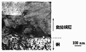
The respective connecting sections were observed by an electron microscope, and when silver microparticles were used, voids were formed on the joint surface with copper. The contact damage of the silver microparticles occurs at the silver/copper interface, and the resulting contact strength of about 5 MPa is considered to be the result of the mechanical connection of the reeds. The contact failure surface of silver nanoparticles is considered to be a trace of silver elongation and plastic deformation, which breaks in the silver layer near the interface (Fig. 8). It can be seen that the interface with silver nanoparticles is stronger than the interface with silver particles.

Figure 8 TEM image of the silver nanoparticle sintered layer/Cu interface
3 Influence of welding parameters on section strength
Figure 9 shows the influence of welding parameters such as welding temperature, welding time and pressure on the cross-section strength of silver nanoparticles. As can be seen from the figure, welding temperature and pressurization are key parameters affecting the strength of the section. In terms of the soldering temperature, the strength rises as the pressurization increases, but in the case where the soldering temperature is high, the influence of the pressurization becomes small. Further, in the case of the welding temperature, when the pressurization is low, the welding temperature has a large influence on the strength, and when the pressurization is increased, the influence of the welding temperature is small. Therefore, it is most effective to increase the pressure at a temperature of about 260 ° C and increase the connection temperature as low as possible.
4 The possibility of dealing with high temperature lead-free soldering
One of the best applications for silver nanoparticle bonding is in high temperature lead-free soldering in the electronics field. In order to achieve lead-free soldering for installation, people have been actively developing new alternatives. The original Sn-Pb eutectic solder (low-to-medium temperature solder) will be replaced by the Sn-Zn system. However, there is currently no suitable substitute for the lead-rich solder used in the package (Pb ≥ 85% Sn-Pb solder).

Fig. 9 The connection strength of silver nanoparticle copper contacts is affected by welding parameters
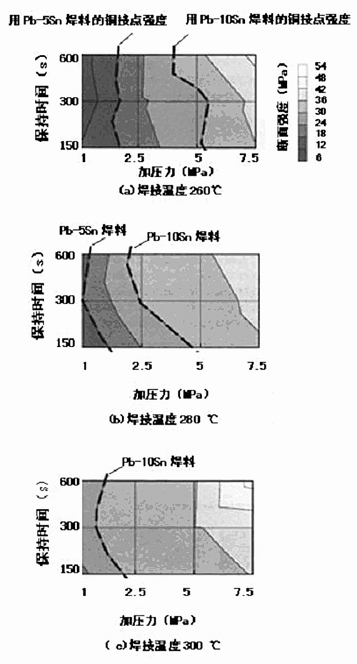
The silver nanoparticle soldering process can be used in the temperature range below the liquid phase temperature (300 ° C, 315 ° C) of the current lead-rich high-temperature solder (260 ° C ~ 300 ° C). Figure 10 is the relationship between the connection conditions and the strength. The dotted line in the figure is the cross-sectional strength of the lead-rich solder Pb-5Sn, Pb-10Sn and Cu disc-type joints (18 MPa, 30 MPa, respectively), and the solid line represents the cross-section strength of the silver nanoparticles. As can be seen from the figure, silver nanoparticles not only have the same strength as Pb-5Sn, but also can be used under wide connection conditions such as low temperature and low pressure. Secondly, whether it is heating or supercharging, the strength of the cross section of silver nanoparticles is unmatched by the other two. Moreover, the joint of the joint has a high melting point, so it does not melt in the subsequent two heat treatments such as welding. In addition, in terms of the electrical conductivity and thermal conductivity required for the chip bonding portion, since the joint is formed of metallic silver, it is necessarily better than the characteristics of the current high-temperature solder.

Fig. 10 Relationship between the connection strength of copper contacts of silver nanoparticles and connection conditions
in conclusion
As a new development in the nanoparticle industry, the silver nanoparticle joining process has a larger range of applications. However, it is also necessary to do a detailed connection mechanism and basic research on connectivity with metals other than Cu. In addition, in terms of practical use of electronic mounting, it is necessary to verify the electrical characteristics and environmental reliability of the joint at a practical level.
12v din rail power supply have 36W and 60W, output current 3A and 5A.
Features:
Wide input range: 100-240V, 50/60Hz.
Easy for the installation and can move in the rail follow CCTV when working
Cooling by free air convection
LED indicator for power on
Protection: short circuit, over current, overload, over voltage.
Efficiency 85%
100% full load burn-in test
3 years warranty
Product application:
Suitable for home automation, CCTV, security camera and led lighting
Din-Rail Power Supply,Din-Rail Power Supply 12Vdc,Din Rail Power Supply Applications,Din Rail Power Supply 48Vdc
Dongguan Xiaoerduo Electronics Co., Ltd. , https://www.steadysmps.com