Key words: LTE230; digital intermediate frequency receiver; digital down conversion; downsampling; filter
CLC number: TN851
Document identification code: A
DOI: 10.16157/j.issn.0258-7998.170880
Chinese citation format: Zhou Chunliang, Zhou Zhimei, Wang Liancheng, et al. Design of LTE230 digital intermediate frequency receiver [J]. Electronic Technology Application, 2017, 43(9): 46-49.
English citation format: Zhou Chunliang, Zhou Zhimei, Wang Liancheng, et al. Design of a digital IF receiver for LTE230 [J]. Application of Electronic Technique, 2017, 43 (9): 46-49.
0 Preface
LTE230 is a dedicated wireless communication system based on TD-LTE advanced technology and customized development in the power industry. The system is deployed in the 223-235 MHz band (230 band). The 230-band resource has a random, comb-like structure, discrete frequency distribution, narrow bandwidth of single-frequency point, and limited transmission capacity. In order to perform high-rate data transmission in power applications, it is necessary to aggregate dozens of frequency points to solve the problem of frequency band resources. Limit problem [1]. The carrier aggregation processing method of the existing LTE-Advanced system is designed for a large-bandwidth, high-rate public network frequency band, and has a large difference in frequency points, frequency bandwidth, and adjacent frequency suppression, and cannot be directly applied to the 230 frequency band; [2] The 230-band IF receiver proposed by LTE-Advanced adopts three independent mixing, mid-band pass filtering and analog-to-digital conversion. It is essentially an analog implementation, with complex hardware structure and reliability to be improved. Not applicable to LTE230 terminal communication module. For the IF signal processing of 230-band carrier aggregation, this paper takes the receiver as an example, and designs a low-cost, high-reliability, high-performance digital IF receiver.
1 230 band spectrum characteristics and LTE 230 frame structure
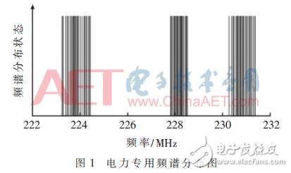
The 230 frequency band is a frequency band used by the National Committee for Telemetry, Remote Control and Data Transmission. It is currently used mainly by the energy, military, water conservancy, geology and mining industries. The total bandwidth of the 230 band is 12 MHz, which is divided into 480 frequency points, each frequency point is 25 kHz, of which 40 frequency points can be used for the power load monitoring system. As shown in Fig. 1, 40 frequency points are divided into 3 clusters. The middle 10 are simplex frequency points, and there are 15 pairs of duplex frequencies on each side [2].
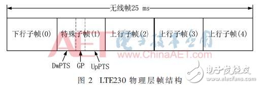
LTE230 is basically the same as TD-LTE in terms of network structure and air interface technology, but the working frequency band and the system can be equipped with a special bandwidth, resulting in a large difference in the physical layer frame structure. As shown in FIG. 2, one radio frame of each frequency point of LTE 230 includes five subframes with a duration of 5 ms, each subframe includes 9 OFDM symbols, and the OFDM symbol uses a 64-point FFT with a subcarrier spacing of 2 kHz. The number of carriers is 10.
2 receiver overall design
2.1 Receiver design principle
Although the frequency band of the 230 frequency band is discrete, in the continuous 12 MHz bandwidth, the total bandwidth is much smaller than that of the LTE-Advanced. The single-band non-continuous carrier aggregation method can be adopted, and the 230-band 12 MHz bandwidth is adopted through one radio frequency unit. The signal is moved to zero frequency as a whole. After analog-to-digital conversion, the intermediate frequency receiving process is performed in the digital domain, and the high-speed intermediate frequency signal with independent bandwidth of 25 kHz dispersed in the 12 MHz bandwidth is converted into a low-speed baseband signal for subsequent signal processing. .
2.2 Overall structure of the receiver
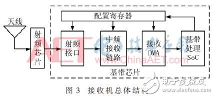
As shown in Figure 3, the receiver is mainly composed of a radio frequency chip and a baseband chip. The radio frequency chip adopts AD9361, embedded analog-to-digital/digital-to-analog converter, and operates in single-port TDD mode, which can be sent and received in time division. A 12-bit parallel digital dual-edge interface based on JESD207 is used between the RF chip and the baseband chip. When receiving, the RF chip generates a 12.8 MHz clock. The I channel data is transmitted on the rising edge of the clock, and the Q channel is transmitted on the falling edge. The main function of the RF interface is to generate the receive control signal and convert the DDR I/Q data of the RF chip digital interface into parallel I/Q data, and complete the conversion from the RF interface 12.8 MHz clock domain to the IF receive link 51.2 MHz clock domain. . The IF receiving link is responsible for extracting the required frequency baseband signal from the intermediate frequency signal and sending it to the system memory through the receiving DMA, and notifying the DSP in the baseband processing SoC to perform subsequent FFT operation, demodulation, decoding, etc. through the interrupt.
2.3 IF Receive Link Design Indicators
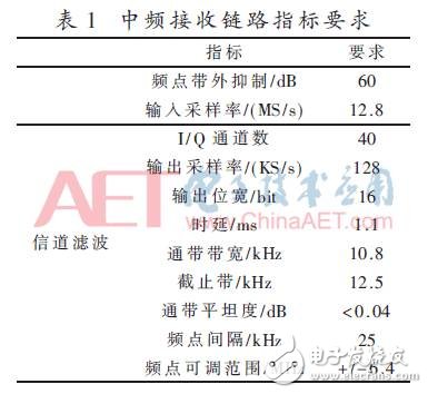
The IF receiving link realizes the conversion of the signal from the intermediate frequency to the baseband by digital down-conversion and decimation filtering. In the above transformation process, the time-frequency domain characteristics of the in-band signal should be kept as constant as possible and the out-of-band noise should be suppressed to the utmost. The IF receiving link is a key component of the receiver performance. According to the LTE 230 specification, the design specification requirements of Table 1 are extracted through system analysis.
2.4 IF receiving link structure
As shown in FIG. 4, the IF receiver data link adopts a two-stage digital down-conversion, down-sampling, and filtering structure, and extracts each frequency point data required from the data received by the radio frequency.

For the spectrum allocation of 40 licensed frequency points of 230-band power, the spectrum allocation is divided into three clusters. The first-stage down-conversion uses three independent numerical control oscillators NCO1 (Numerically Controlled Oscillator) to move each cluster as a whole to zero frequency. NCO1 is followed by a half-band filter HBF (Half Band Filter) for 2x extraction (12.8 ~ 6.4 MS / s) and high-frequency component filtering.
The two-stage down-conversion uses 40 independent numerical control oscillator NCO2 to move the required frequency point signal from three clusters to zero frequency to realize the extraction of the desired frequency point signal. The frequency point data output by the NCO2 is subjected to 50 times of decimation filtering (6.4 to 128 KS/s) by a cascaded integrator comb filter CIC (Cascaded Integrator Comb). After the CIC, a high-order low-pass filter LPF (Low Pass Filter) is cascaded to suppress the out-of-band signal of each frequency point.
3 IF receiving link module design
3.1 Module design method
The IF receive link filter is designed and analyzed using MATLAB's fdatool, which is decomposed according to the link index to determine the order, coefficient and bit width of each filter. In the design of the corresponding digital circuit RTL, considering that the LTE230 private network is still in the process of continuous development, and the difference in bandwidth requirements of different application scenarios, while leaving a certain performance margin, the frequency points, the NCO carrier frequency, the HBF and The LPF order and coefficients can be flexibly configured through software.
3.2 Numerically Controlled Oscillator NCO
In LTE230, the received intermediate frequency signal has I/Q two-way, and the down-conversion principle is as shown in equation (1). Down-conversion can be realized by multiplying the sine and cosine local oscillator signals by the NCO and multiplying the received signal by the phase accumulation.

The NCO1 and NCO2 work frequency points can be matched with an accuracy of 25 kHz (Δf), and the structure is the same. The sampling rate corresponding to NCO1 is 12.8 MS/s (Fs), the phase accumulated word width is 9 bits (2N=Fs/Δf); the sampling rate of NCO2 is 6.4 MS/s, and the phase accumulated word width is 8 bits. The NCO1 and NCO2 sine and cosine carriers are implemented by means of a look-up table. The look-up table only needs to store the sine and cosine values ​​in the π/4 angle. Others can be obtained by sine-cosine transformation or symbol conversion look-up table. The lookup tables corresponding to NCO1 and NCO2 are positive. The cosine values ​​are 64 and 32 respectively, and the bit width is 16 bits. The multiplication of the complex number in the downconversion requires 4 multiplication operations. Since the operating clock frequencies of NCO1 and NCO2 are 4 times and 8 times the sampling rate, time division multiplexing is used, and only one multiplier is required.
3.3 Half Band Filter HBF
HBF is a special FIR filter whose passband and stopband are symmetric and equal in width with respect to 1/2 of the Nyquist frequency. The HBF impulse response is:

It can be seen from equation (2) that the HBF impulse response is zero at all other even points except that it is 1 at the h(0) zero point. Compared with the ordinary 2 times extraction FIR, the coefficients are not only symmetric but also Nearly half of the zeros can reduce the amount of filtering operations by half.
The default passband bandwidth of HBF is 2 MHz, the maximum order can be 25th order, the stopband rejection is 78 dB, the coefficient is quantized to 16 bits, the coefficient is symmetric about the center tap (1/2), and the effective coefficient is only 6. It is necessary to perform 6 multiplication operations. The HBF working clock frequency is 8 times of the output sampling rate. It is realized by time division multiplexing, and one multiplier of I/Q two channels can be realized.
3.4 Cascade Integral Comb Filter CIC
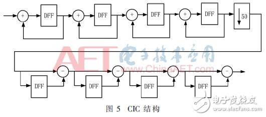
CIC is an effective interpolation and decimation filter widely used in multi-rate digital signal processing. The first sidelobe suppression of single-stage CIC is 13.46 dB, and the stopband attenuation is extremely unsatisfactory [3]. In practical applications, cascaded is often used, but the cascade is generally not more than 5, otherwise the distortion in the passband will be Increase. In LTE230, the 4-level CIC is used, and the decimation factor is 50 (N=4, R=50). The specific structure is shown in Figure 5. As can be seen from the figure, the CIC structure is very simple, consisting of an integrator and a comb filter. The corresponding sampling rates are 6.4 MS/s and 128 KS/s, respectively. It can be realized by adder, subtractor and delay register (DFF). There is no multiplication operation, the area is small and the processing speed can be high. .
Passband attenuation is one of the main drawbacks of CIC, usually in the time domain plus compensation filter for passband compensation [4]. Considering that the 230-band frequency effective bandwidth is very narrow and the OFDM system is not very sensitive to passband flatness, interpolation compensation is performed in the frequency domain by channel estimation of the reference signal in LTE230.
3.5 Low Pass Filter LPF
LPF is the final stage of decimation filtering. While ensuring the flatness of the passband, the sidelobe amplitude of the CIC is minimized and the stopband attenuation is accelerated. At the same time, in order to realize the coexistence of LTE230 and the traditional 230-band digital radio station, the out-of-band rejection must be 65 dB according to the requirements of the digital radio station [5].
At design time, the LPF can be ordered with a maximum order of 255 steps, a default passband bandwidth of 10.8 kHz, a stopband bandwidth of 12.5 kHz, a ripple factor of 0.02 dB, and a stopband rejection of 65 dB. The LPF coefficient is quantized to 18 bits, the coefficients are symmetric and configurable, and the 255-order LPF I/Q data requires 128 multiplication operations. Considering that the LPF operating clock frequency is 400 times the sampling rate, I/Q data and computing resources can be used. The time division multiplexing structure can be realized by only one multiplier and a small number of adders, which greatly saves circuit resources.
4 Simulation and FPGA verification
4.1 Simulation verification
The LTE230 baseband processing is very complicated. To simplify the simulation verification, different frequency sine and cosine waves are used instead of the LTE230 IF signal. The processing of 40 frequency points is the same, only one of them is simulated. The MATLAB simulation parameters are set as follows:
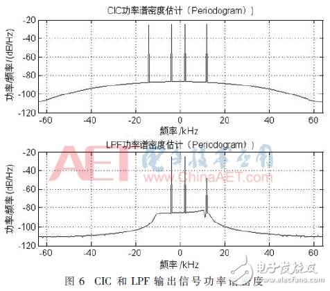
The NCO1 local oscillator frequency is 2 MHz (80 × 25 kHz), and the NCO2 local oscillator frequency is 125 kHz (5 × 25 kHz), corresponding to the 230-band 231.125 MHz (RF center frequency 229). The intermediate frequency inputs 4 complex signals (cos(2πft)+jsin(2πft)), and the frequencies f are 2.111 MHz, 2.121 MHz, 2.127 MHz, and 2.137 MHz, respectively. It is calculated that there are 4 frequencies after NCO1 and HBF: 0.111 MHz, 0.121 MHz, 0.127 MHz and 0.137 MHz. There are 4 frequencies after NCO2 and CIC: -14 kHz, -4 kHz, 2 kHz and 12 kHz, due to LPF The passband is 10.8 kHz and the stopband is 12.5 kHz. After LPF, the -4 kHz, 2 kHz signal is unchanged, the -14 kHz signal is filtered out, and the 12 kHz signal is attenuated. Figure 6 shows the signal power spectral density of the CIC and LPF simulation outputs. It can be seen from the figure that the simulation results are consistent with the calculated values. The simulation results of NCO1, HBF and NCO2 are also consistent with the theoretical values, which are not listed due to space reasons. The overall simulation results show that the implementation method of the digital intermediate frequency receiver proposed in this paper is feasible.
After the MATLAB simulation is passed, the input and output of each node are imported into the RTL verification platform for simulation. The RTL code and the fixed-point algorithm are precisely matched, and the correctness is ensured through data comparison.
4.2 FPGA verification
Limited by the speed of the FPGA device, the baseband processing SoC cannot run at full speed, and the complete LTE230 system test cannot be performed. It mainly tests the tone signal and the LTE230 resident process. The single tone test is similar to the simulation. The single tone signal generated by the signal generator is sent to the intermediate frequency for processing by RF down-conversion, and the processing result is imported into MATLAB for waveform and spectrum analysis. The LTE 230 camping process is a necessary process for establishing a connection with the base station after the terminal is powered on, including steps of cell search and broadcast information reception. Since the number of effective subcarriers in the 230-band single-frequency point is only 10, the primary synchronization signal, the secondary synchronization signal, and the broadcast channel used in the camping process must occupy all the effective subcarriers in multiple OFDM symbols, so this is a typical intermediate frequency. Receiving the performance test scenario, the measured results show that the sensitivity of the resident process is as high as -124 dBm, which fully meets the system requirements.
5 Conclusion
In this paper, an all-digital IF receiver is designed for the 230-band characteristics and LTE230 system requirements. It uses two-stage digital down-conversion and high-order digital filters to effectively solve the problem with smaller circuit area by time division multiplexing. The 230 frequency band has many frequency points, distributed dispersion, and high requirements for adjacent frequency suppression. It achieves the aggregation of 40 frequency points in the 230 frequency band, which can meet the data transmission requirements of high-rate power applications. The digital IF receiver has been successfully applied to the LTE230 wireless communication baseband chip [1] after MATLAB algorithm design and simulation, RTL simulation and FPGA verification. Currently, the chip-based communication module has been running stably for more than two years in the pilot project. The functional performance indicators are good and fully meet the practical application requirements, which fully demonstrates that the design of the digital IF receiver is successful.
2G GPS Tracker,2G GPS Trackers,3G GPS Tracker, 2G Vehicle GPS Trackers,3G GPS Trackers
eSky wireless Inc , https://www.eskygpsiot.com